Semiconductor circuit

a technology of semiconductors and circuits, applied in the direction of semiconductor devices, basic electric elements, electrical equipment, etc., can solve the problems of large chip area consumed by laterally oriented devices, 64-bit computer chips will need more devices, and require expensive advances in lithography and manufacturing equipmen

Inactive Publication Date: 2011-03-03
BESANG
View PDF100 Cites 222 Cited by
  • Summary
  • Abstract
  • Description
  • Claims
  • Application Information

AI Technical Summary

Problems solved by technology

However, these laterally oriented devices consume significant amounts of chip area.
However, the 64-bit computer chip will need more devices since there are more bits to process at a given time.
The number of devices can be increased by making the devices included therein smaller, but this requires expensive advances in lithography and manufacturing equipment.
However, the yield of the computer chips fabricated in a run decreases as their area increases, which increases the overall cost.
However, there are several

Method used


Image

  • Semiconductor circuit
  • Semiconductor circuit
  • Semiconductor circuit

Examples


Embodiment Construction

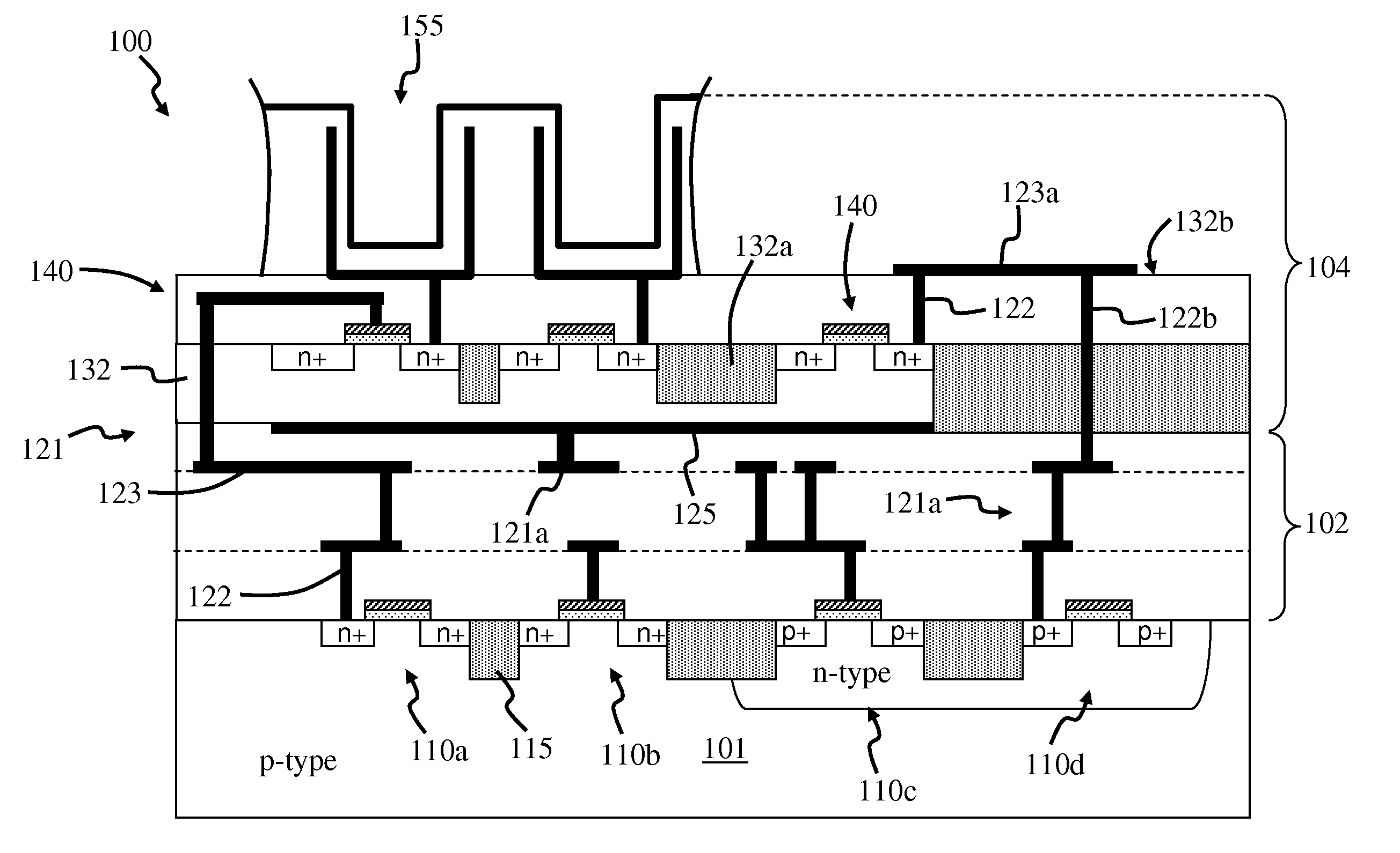
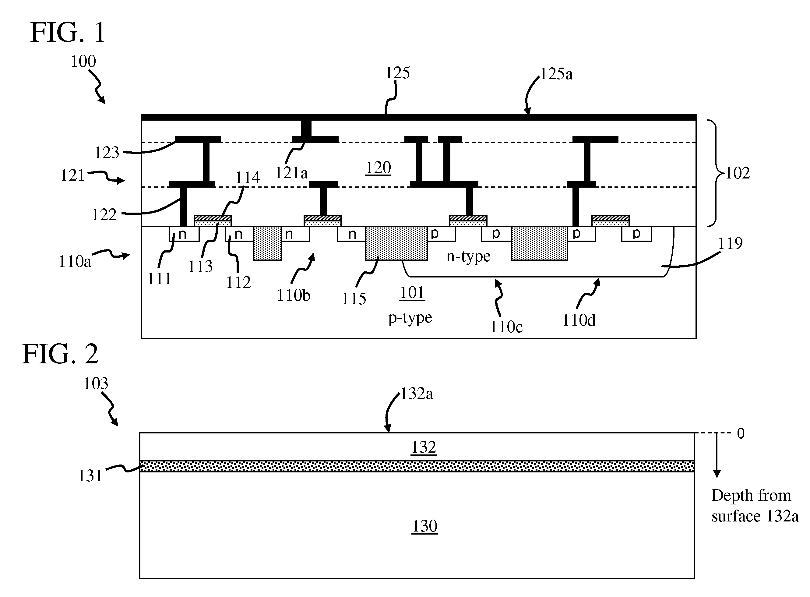
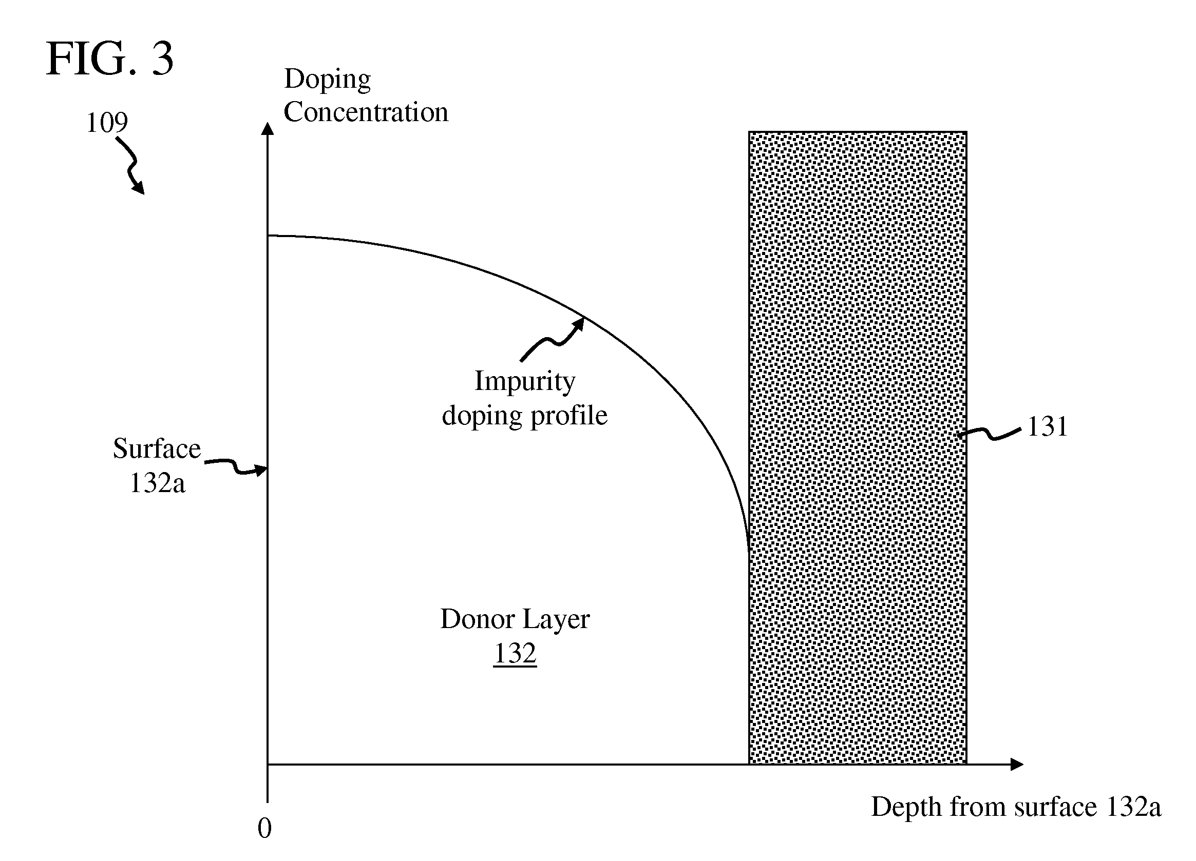
FIGS. 1-9 are sectional views of steps in forming a semiconductor circuit 100. Semiconductor circuit 100 can be included in a computer chip having a memory region carried by a carrier substrate, wherein the carrier substrate generally has electronic circuitry formed therewith. The carrier substrate is typically a semiconductor substrate, which includes a semiconductor material such as silicon.

In some embodiments, the electronic circuitry formed with the carrier substrate includes processor and / or control circuitry. The processor circuitry processes data, such as digital data, and the control circuitry controls the flow of the data, such as sending it to and retrieving it from the memory region. The electronic circuitry can include many different types of electronic devices, such as metal-oxide semiconductor field effect transistors (MOSFET). One type of electronic circuitry often used is referred to as complementary MOSFET (CMOS) circuitry.

The memory region can include many differen...


PUM


Abstract

A semiconductor memory device includes a substrate and an interconnect region carried by the substrate. A donor layer is coupled to the interconnect region through a bonding interface. An electronic device is formed with the donor layer, wherein the electronic device is formed after the bonding interface is formed. A capacitor is connected to the electronic device so that the electronic device and capacitor operate as a dynamic random access memory device.

Description

BACKGROUND OF THE INVENTION1. Field of the InventionThis invention relates to semiconductor circuits formed using wafer bonding.2. Description of the Related ArtAdvances in semiconductor manufacturing technology have provided computer chips with integrated circuits that include many millions of active and passive electronic devices, along with the interconnects to provide the desired circuit connections. As is well-known, most integrated circuits include laterally oriented active and passive electronic devices that are carried on a single major surface of a substrate. Active devices typically include transistors and passive devices typically include resistors, capacitors, and inductors. However, these laterally oriented devices consume significant amounts of chip area.It is desirable to provide computer chips that can operate faster so they can process more data in a given amount of time. The speed of operation of a computer chip is typically measured in the number of instructions p...

Claims


Application Information

Patent Timeline
IPC IPC(8): H01L21/02
CPCH01L21/2007H01L2924/01033H01L24/83H01L27/0688H01L2224/291H01L2224/8385H01L2924/01013H01L2924/01015H01L2924/01042H01L2924/01073H01L2924/01074H01L2924/07802H01L2924/13091H01L2924/14H01L2924/19041H01L2924/19042H01L2924/19043H01L24/29H01L2924/01006H01L21/8221
Inventor LEE, SANG-YUN
Owner BESANG
Why Eureka
Try Eureka