
Gas mixing method realized by back diffusion in a pecvd system with showerhead

a technology of back diffusion and gas mixing, which is applied in the direction of chemical vapor deposition coating, coating, plasma technique, etc., can solve the problems of reducing the conversion efficiency of pv solar cells, increasing production costs, and reducing manufacturing throughpu

Inactive Publication Date: 2011-03-03
APPLIED MATERIALS INC
View PDF7 Cites 8 Cited by
  • Summary
  • Abstract
  • Description
  • Claims
  • Application Information

AI Technical Summary

Problems solved by technology

Insufficient crystallinity of the silicon film for layers that should be microcrystalline or polycrystalline may cause incomplete formation and fraction of the film, thereby reducing the conversion efficiency in a PV solar cell.
Additionally, conventional deposition processes of microcrystalline silicon film have slow deposition rates, which disadvantageously reduce manufacturing throughput and increase production costs.

Method used


Image

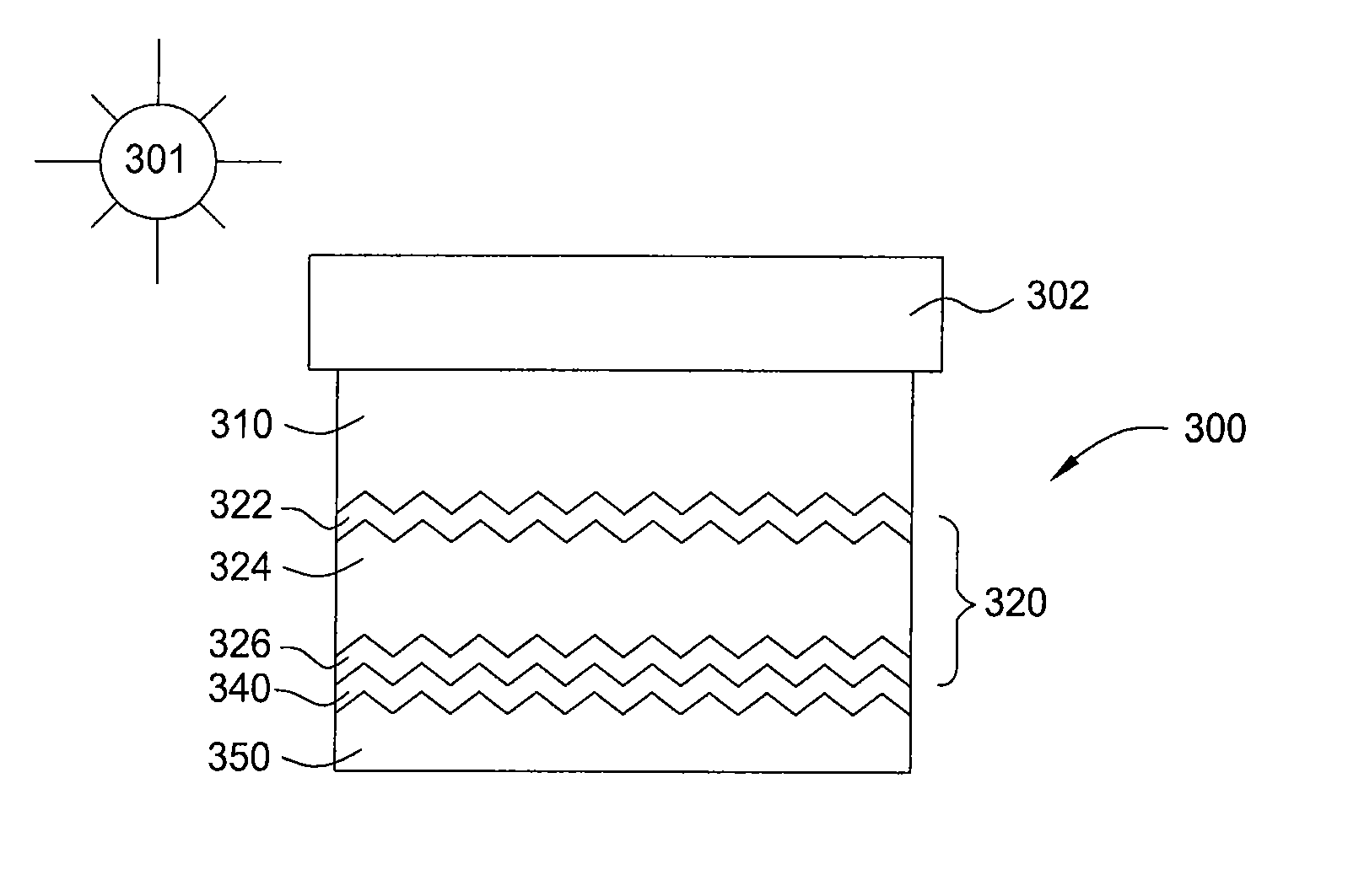
  • Gas mixing method realized by back diffusion in a pecvd system with showerhead
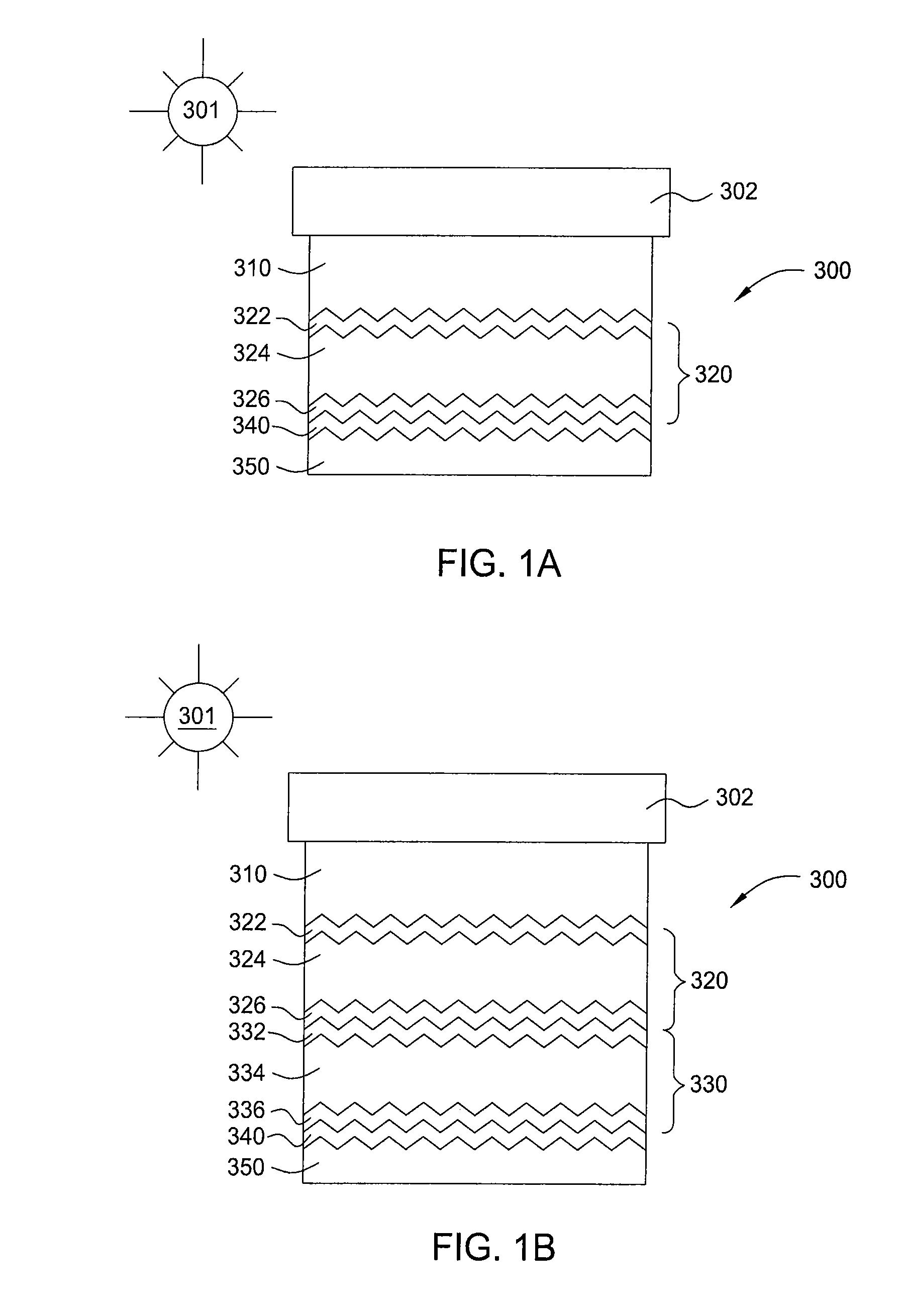
  • Gas mixing method realized by back diffusion in a pecvd system with showerhead
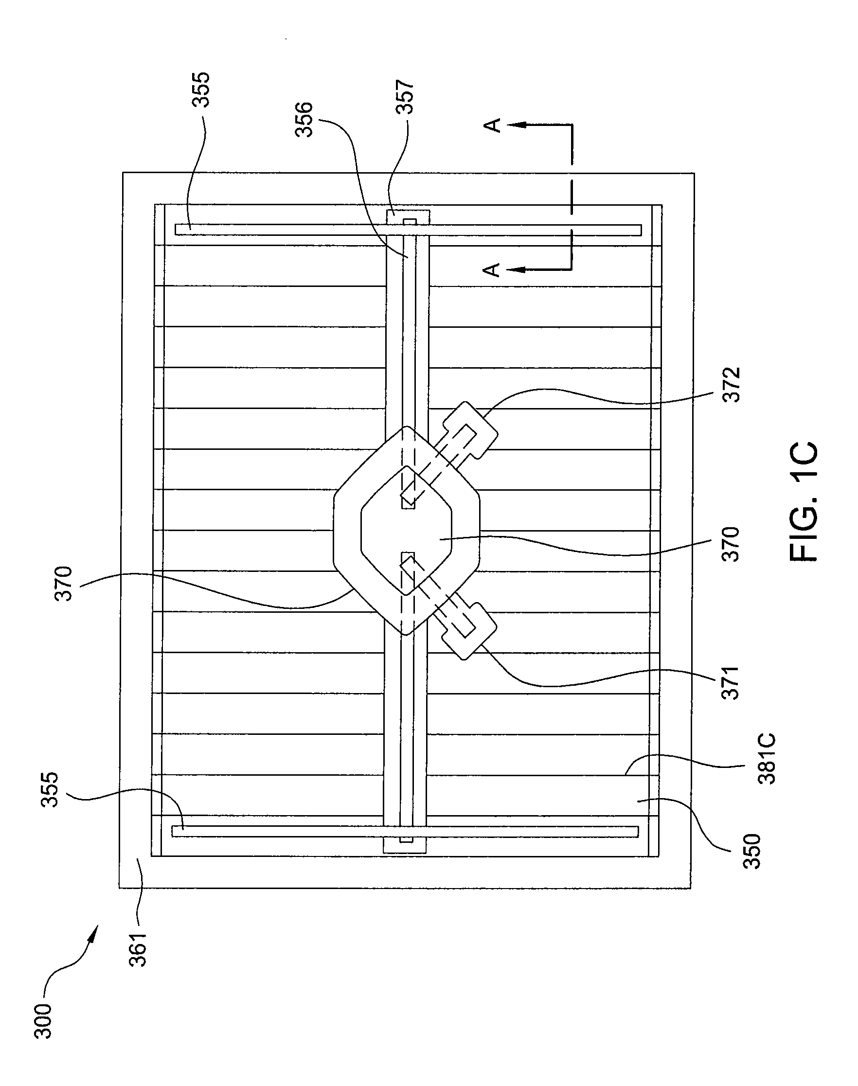
  • Gas mixing method realized by back diffusion in a pecvd system with showerhead

Examples


example 1

[0060]Table 1 shows various deposition parameters for a conventional-type method of forming microcrystalline silicon on a substrate. A 600×720 mm substrate is processed in a PECVD chamber, such as the AKT 4300 PECVD systems available from Applied Materials, Inc. In this conventional type method, pure silane was flown into the chamber without a carrier gas or hydrogen gas.

[0061]Each sample was placed in a chamber with a spacing of 640 millimeters between the showerhead and the substrate. The silane gas flow rate and pressures varied for each sample, as well as the power setting for forming the plasma. The deposition process was carried out at around 200° C. Each of the samples were processed for 600 seconds.

TABLE 1FlowPressureSpacingPowerSample(sccm)(Torr)(millimeters)(W)D-Si-x1618056403000D-Si-x1718096403000D-Si-x189096402000

[0062]FIGS. 6A-6C illustrate the crystallinity test results from the various samples listed in and processed according to Table 1. 70×100 mm coupons from the 60...

example 2

[0064]Table 2 shows various deposition parameters according to embodiments of the invention for forming microcrystalline silicon on a substrate. Without a hardware change, various process parameters were changed along with performing the cycling of the process gas. A 600×720 mm substrate is processed in a PECVD chamber, such as the AKT 4300 PECVD systems available from Applied Materials, Inc. In the xy ‘908A5 sample, the pressure was maintained to be around 6-8 Torr, which was achieved by opening and closing the gate valve of the pump exhaust system. Additionally, the silane gas flow was increased to about 2500 sccm and flown into the chamber without a carrier gas. The power setting was increased to 5000 watts when striking a plasma. During the processing of each sample, the power remained on to maintain the plasma,

[0065]The flow of silane into the chamber was cycled according to the parameters listed in Table 2. The silane gas was on for 5 seconds of a 60-second cycle. During the 5...


PUM

PropertyMeasurementUnit
RF poweraaaaaaaaaa
sizeaaaaaaaaaa
frequencyaaaaaaaaaa

Abstract

Embodiments of the present invention generally relate to methods of forming a microcrystalline silicon layer on a substrate in a deposition chamber. In, one embodiment, the method includes flowing a processing gas into a diffuser region between a backing plate and a showerhead of the deposition chamber, flowing the processing gas through a plurality of holes in the showerhead and into a process volume between the showerhead and a substrate support in the deposition chamber, igniting a plasma in the process volume, back-flowing gas ions formed in the plasma through the plurality of holes in the showerhead and into the diffuser region, mixing the gas ions and the processing gas in the diffuser region, re-flowing the gas ions and processing gas through the plurality of holes in the showerhead and into the process volume, and depositing a microcrystalline silicon layer on the substrate.

Description

CROSS-REFERENCE TO RELATED APPLICATIONS[0001]This application is related to U.S. application Ser. No. 12 / 202,199, filed Aug. 29, 2008 (Attorney Docket No. APPM / 11141), U.S. application Ser. No. 12 / 201,840, filed Aug. 29, 2008 (Attorney Docket No. APPM / 11141.02), and U.S. application Ser. No. 11 / 426,127, filed Jun. 23, 2006 (Attorney Docket No. APPM / 010953).BACKGROUND OF THE INVENTION[0002]1. Field of the Invention[0003]Embodiments of the present invention generally relate to thin-film formation, such as for solar cells, and methods for forming thin-films. More particularly, embodiments of the present invention relate to methods of forming an intrinsic-type silicon layer having mixed silicon phases formed in thin-film and crystalline solar cells.[0004]2. Description of the Related Art[0005]Photovoltaic (PV) devices or solar cells are devices which convert sunlight into direct current (DC) electrical power. Crystalline silicon solar cells and thin-film solar cells are two types of sol...

Claims


Application Information

Patent Timeline
Patent Type & Authority Applications(United States)
IPC IPC(8): H01L21/205
CPCC23C16/24C23C16/452C23C16/45512C23C16/45565H01J37/32091H01L21/0262H01J37/3244H01J37/32449H01L21/02532H01L21/02595H01J37/32357
Inventor YANG, XIESENCHAE, YONG-KEESHENG, SHURANLI, LIWEI
Owner APPLIED MATERIALS INC
Learn More