Method of manufacturing semiconductor device and substrate processing apparatus

a technology of substrate processing and semiconductor devices, which is applied in the direction of semiconductor devices, liquid surface applicators, coatings, etc., can solve the problems of difficult control of the concentration of atomic oxygen o in the stacked direction of wafers and prevent the reverse loading

Inactive Publication Date: 2011-03-17
KOKUSA ELECTRIC CO LTD
View PDF10 Cites 12 Cited by
  • Summary
  • Abstract
  • Description
  • Claims
  • Application Information

AI Technical Summary

Benefits of technology

[0018]According to another aspect of the present invention, there is provided a substrate processing apparatus including: a process chamber configured to process a plurality of substrates by oxidation; a holding tool configured to hold the substrates in the process chamber; a mixing part configured to mix an oxygen-containing gas and a hydrogen-containing gas and supply the mixture from an end side of a substrate arrangement region where the substrates are arranged inside the process chamber; a nozzle configured to supply a hydrogen-containing gas from a plurality of mid-flow locations corresponding to the substrate arrangement region inside the process chamber; an exhaust outlet configured to exhaust an inside of the process chamber so that the gases supplied into the process chamber flow toward the

Problems solved by technology

In addition, according to the study of the inventors, in the above-described method (such as a method of supplementarily supplying H2 gas through sub

Method used


Image

  • Method of manufacturing semiconductor device and substrate processing apparatus
  • Method of manufacturing semiconductor device and substrate processing apparatus
  • Method of manufacturing semiconductor device and substrate processing apparatus

Examples


embodiment of invention

[0061]Hereinafter, an explanation will be given on an embodiment of the present invention based on the above-described knowledge of the inventors with reference to the attached drawings.

[0062](1) Structure of Substrate Processing Apparatus

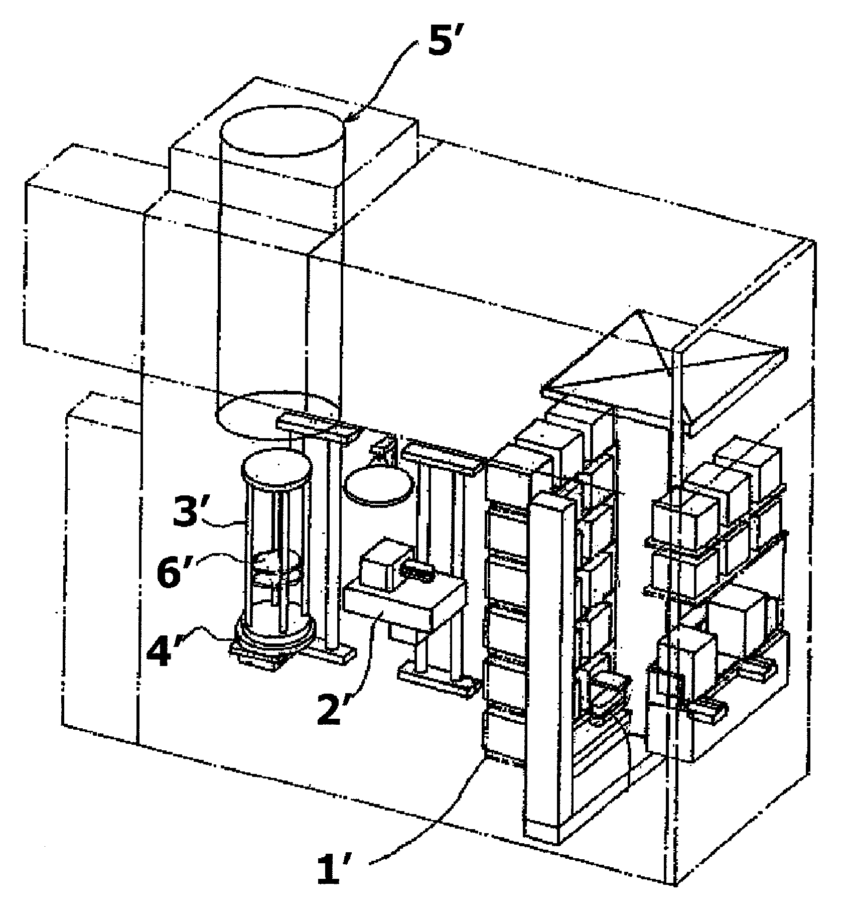
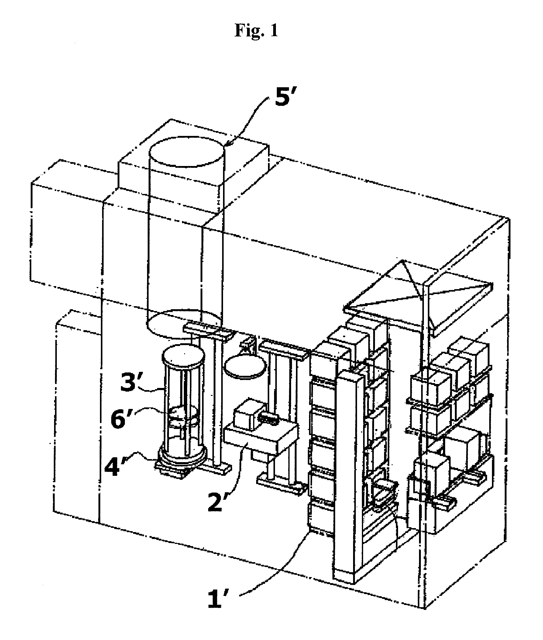
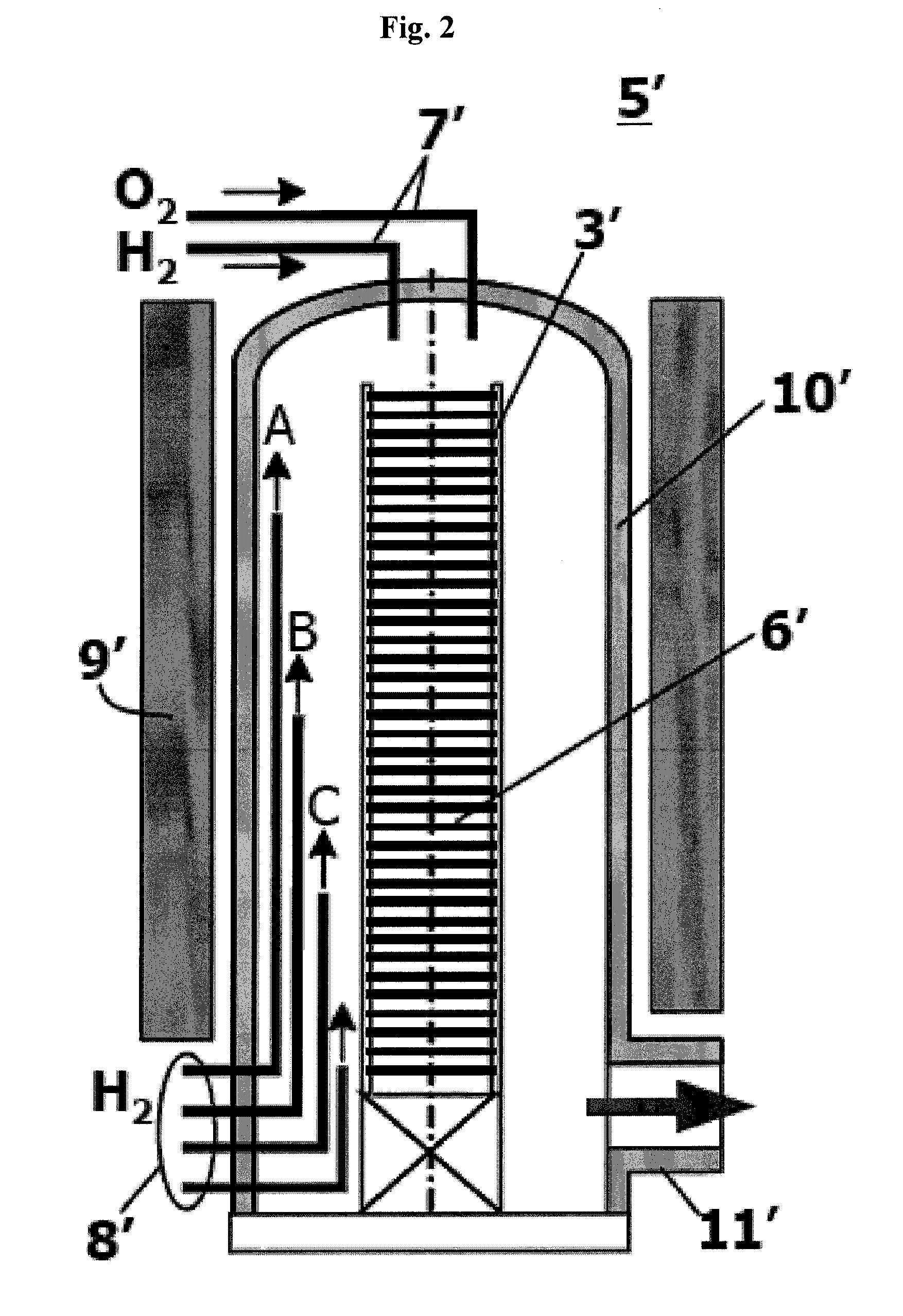
[0063]First, as a substrate processing apparatus in accordance with an embodiment of the present invention, a batch-type vertical semiconductor manufacturing apparatus (oxidation apparatus) will be described with reference to FIG. 7. FIG. 7 is a schematic sectional view showing a configuration example of a heat-treating furnace (oxidation furnace) relevant to the current embodiment of the present invention. FIG. 7 illustrates an exemplary structure of a heat-treating furnace 5 of a substrate processing apparatus whose maximum loading capacity is for example 120 wafers.

[0064]As shown in FIG. 7, the heat-treating furnace 5 of the substrate processing apparatus relevant to the current embodiment includes a heater 9 as a heat source. The heater 9 is cy...


PUM


Abstract

At a low temperature of 500° C. to 700° C., the concentration of atomic oxygen is controlled in a wafer stacked direction, and the thickness distribution of oxide films is kept uniform in the wafer stacked direction. A semiconductor device manufacturing method includes a process of oxidizing substrates by supplying oxygen-containing gas and hydrogen-containing gas through a mixing part from an end side of a substrate arrangement region where the substrates are arranged inside the process chamber so that the gases flow toward the other end side of the substrate arrangement region, and supplying hydrogen-containing gas from mid-flow locations corresponding to the substrate arrangement region. The oxygen-containing gas and the hydrogen-containing gas reacts with each other in the mixing part to produce an oxidation species containing atomic oxygen, and the oxidation species has a maximum concentration at an ejection hole through which the oxidation species is ejected from the mixing part into the process chamber.

Description

CROSS-REFERENCE TO RELATED PATENT APPLICATION[0001]This U.S. non-provisional patent application claims priority under 35 U.S.C. §119 of Japanese Patent Application No. 2009-215750, filed on Sep. 17, 2009, in the Japanese Patent Office, the entire contents of which are hereby incorporated by reference.BACKGROUND OF THE INVENTION[0002]1. Field of the Invention[0003]The present invention relates to a substrate processing apparatus and a method of manufacturing a semiconductor device which includes a process of treating a substrate by using the substrate processing apparatus, and more particularly, to an oxidation apparatus configured to oxidize a surface of a substrate and a method of manufacturing a semiconductor device such as an integrated circuit (IC) which includes a process of oxidizing a substrate using the oxidation apparatus.[0004]2. Description of the Related Art[0005]FIG. 1 is an overall view of an apparatus for manufacturing a semiconductor device (semiconductor manufacturi...

Claims


Application Information

Patent Timeline
IPC IPC(8): H01L21/71B05C11/00B05C21/00
CPCH01L21/02233H01L21/02238H01L29/7881H01L21/28273H01L21/67109H01L21/02255H01L29/40114H01L21/0223H01L21/02263H01L21/67248
Inventor SASAKI, TAKAFUMIFUKUDA, MASANAOMINAMI, MASAYOSHIMEGAWA, YASUHIRO
Owner KOKUSA ELECTRIC CO LTD
Why Eureka
Try Eureka