Electronic device and method of manufacturing an electronic device

a manufacturing method and electronic technology, applied in the field of electronic devices, can solve problems such as inconvenience in the process, antenna production, and the need for several steps in the antenna production process

Inactive Publication Date: 2011-03-31
NXP BV
View PDF65 Cites 7 Cited by
  • Summary
  • Abstract
  • Description
  • Claims
  • Application Information

AI Technical Summary

Benefits of technology

[0016]According to the invention the electronic device comprises an integrated circuit embedded into a substrate, wherein the substrate has at least a first and a second conductive structure arranged on opposite sides of the integrated circuit and the electrical connections between the first and the second conductive structure and / or with the integrated circuit are established by means of holes in the substrate. By having a configuration, where the integrated circuit as well as the first and the second conductive structure are arranged and realized in the substrate, a particularly compact design is achieved, wherein the integrated circuit is totally protected from external impacts. Because the first and the second conductive structure are arranged on opposite sides of the integrated circuit it is feasible to have, e.g., antenna structures arranged directly on or in the substrate, whereby it is of particular advantage, if, in accordance with a preferred embodiment of the invention, the first conductive structure forms a conductive bridge between two regions of the second conductive structure. Thus, one of the conductive structures can form the antenna and the other conductive structure, being on the opposite side of the integrated circuit, can form the bridge to connect two distant ends or regions of the antenna. The bridge is just realized as an additional layer in the substrate and does not significantly add to the complexity of the design. At the same time, the bridging layer can serve to add stability to the substrate and can function as a protective layer for the integrated circuit. In particular, the bridging layer can serve to protect the integrated circuit from light exposure during production.
[0042]As in accordance with a preferred embodiment of the present invention, said step of forming the second conductive structure comprises applying at least one conductive trace on the substrate in a spiral like form, which allows for an efficient use of the space available on the substrate. Preferably, the second conductive structure forms an antenna, such as an antenna for RFID applications. In this case, the first conductive structure serves as a bridge for connecting the two ends of the coil-like antenna.

Problems solved by technology

In such a process, the step of providing the antenna structure on a surface of the substrate layer and the step of contacting the antenna structure with the chip are separate, thereby giving rise to procedural inconvenience.
Structures using direct chip attach reveal the disadvantage that the IC is more or less unprotected during the lamination process, which limits the IC thickness to around 100 μm in order to give reasonable die strength values.
Another problem is the antenna production, and in particular the establishing of a bridge for connecting the two ends of the antenna.
The common problem to all manufacturing methods as described above is that the antenna production process requires several steps.
In case an interposer or moduler is used, the manufacturing process is even more complicated, because also additional interconnects between the integrated circuit and the leads and between the leads and the antenna have to be made.
Especially for the realization of ultra-thin inlays or prelams the handling of thin integrated circuits is difficult.
Additionally, thin integrated circuits are known to be light sensitive, so that protective layers may have to be applied.

Method used


Image

  • Electronic device and method of manufacturing an electronic device
  • Electronic device and method of manufacturing an electronic device
  • Electronic device and method of manufacturing an electronic device

Examples


Embodiment Construction

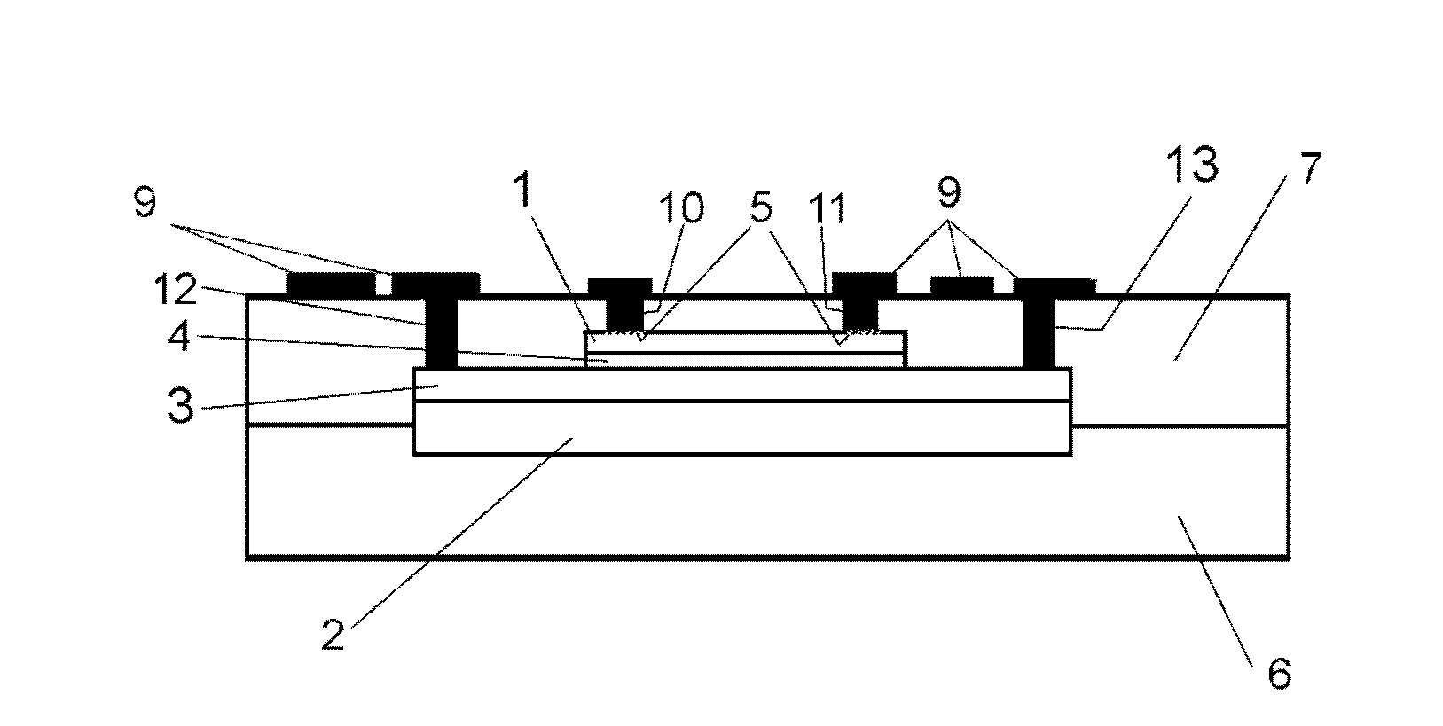
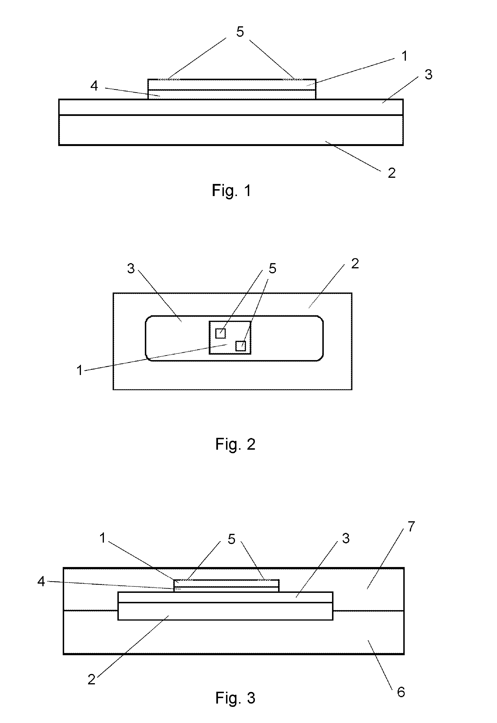
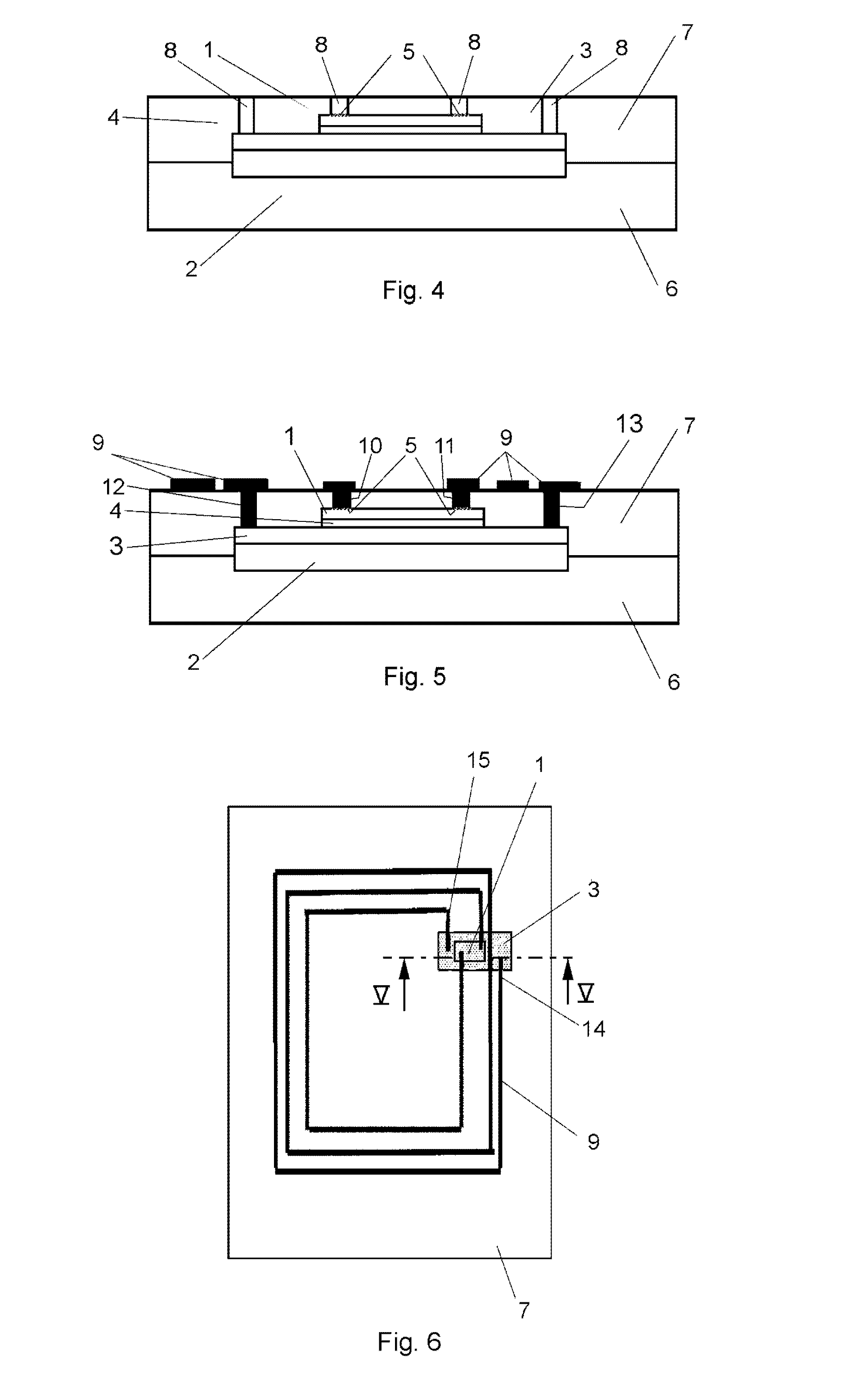
[0052]In FIG. 1, an IC 1, by interposition of an isolating layer 4, is in a first process step placed on a first conductive structure, which in this case is a conductive layer 3 arranged on a carrier 2, such as a polymer carrier. The isolating layer 4 also functions as an adhesive for firmly holding the IC 1 on the conductive layer 3. From a process point of view the handling of the IC 1 being fixed onto the carrier 2 is much easier than a direct pick and place process and can be easily integrated into an antenna production and lamination environment. This first process step is similar to IC packaging for an interposer, but without the need of a metal interconnection between the IC and the conductive parts of the carrier and much relaxed positioning tolerances. In the top view according to FIG. 2 it can be seen that the conductive layer 3 can be patterned in a way to optimize the following process steps. In particular it will be realized that the exact positioning of the IC 1 on the...


PUM

PropertyMeasurementUnit
thicknessaaaaaaaaaa
thicknessaaaaaaaaaa
conductiveaaaaaaaaaa

Abstract

Electronic device comprising an integrated circuit (1) embedded into a substrate, wherein the substrate has at least a first (3) and a second (9) conductive structure arranged on opposite sides of the integrated circuit (1) and the electrical connections (10,11,12,13) between the first (3) and the second (9) conductive structure and / or with the integrated circuit 5 (1) are established by means of holes (8) in the substrate.

Description

FIELD OF THE INVENTION[0001]The invention relates to an electronic device comprising an integrated circuit embedded into a substrate.[0002]Further, the invention relates to a method of manufacturing an electronic device.BACKGROUND OF THE INVENTION[0003]Electronic devices within the scope of the present invention and in particular smartcards for radio frequency identification (RFID) applications usually consist of an integrated circuit (IC), packaged in a module, which is then connected with an antenna and subsequently integrated into a cardbody. For standard cards, normally the module is attached to a substrate foil, in which the insulated wire antenna is embedded and attached by a welding process to the module. This substrate foil then is called an inlay, which, in a separate step, is laminated into the final RFID card.[0004]An alternative way of producing an inlay uses a so-called direct chip attach process. In that case, the antenna consists of a structured layer of a conductive ...

Claims


Application Information

Patent Timeline
Patent Type & Authority Applications(United States)
IPC IPC(8): H05K1/09H05K1/16H05K3/36
CPCG06K19/07749Y10T29/49126H01L23/5389H01L24/18H01L24/82H01L2224/18H01L2224/82039H01L2224/82047H01L2924/01033H01L2924/01082H01L2924/14H01L2924/01023H01L2924/014H01L2224/32145H01L2224/73267H01L23/49855H01L2224/04105H01L2223/6677H01L2224/32225H01L2224/32245H01L2224/92244H01L24/24
Inventor ZENZ, CHRISTIAN
Owner NXP BV
Why Eureka
Try Eureka