

Methods for a gate replacement process
- Summary
- Abstract
- Description
- Claims
- Application Information
AI Technical Summary
Benefits of technology
Problems solved by technology
Method used
Image

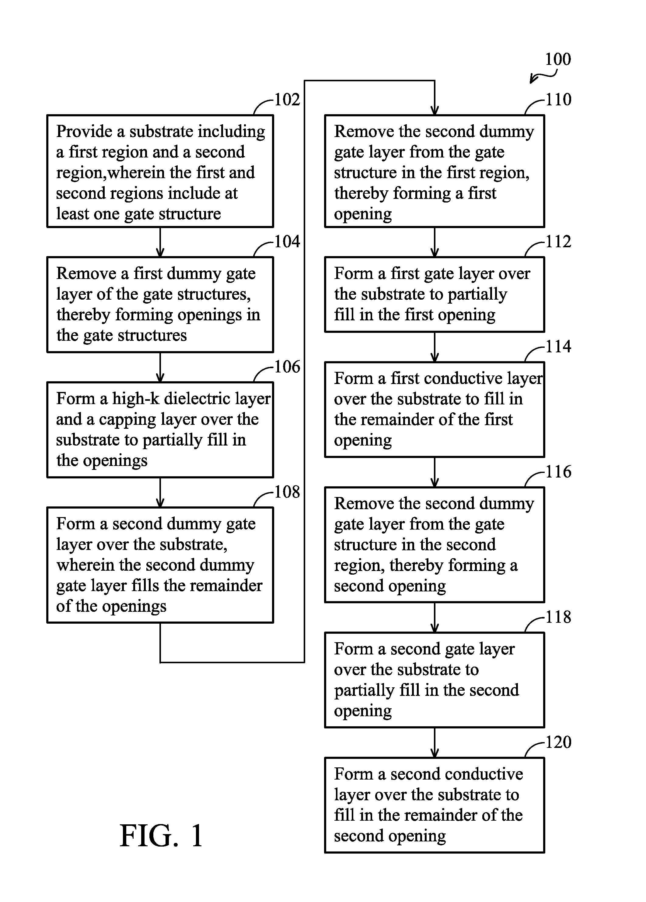
Examples
Embodiment Construction
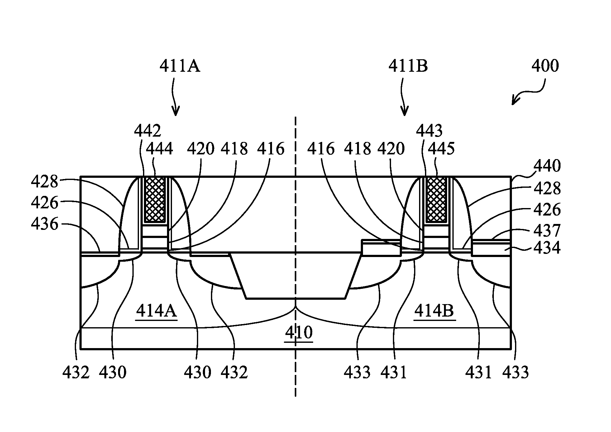
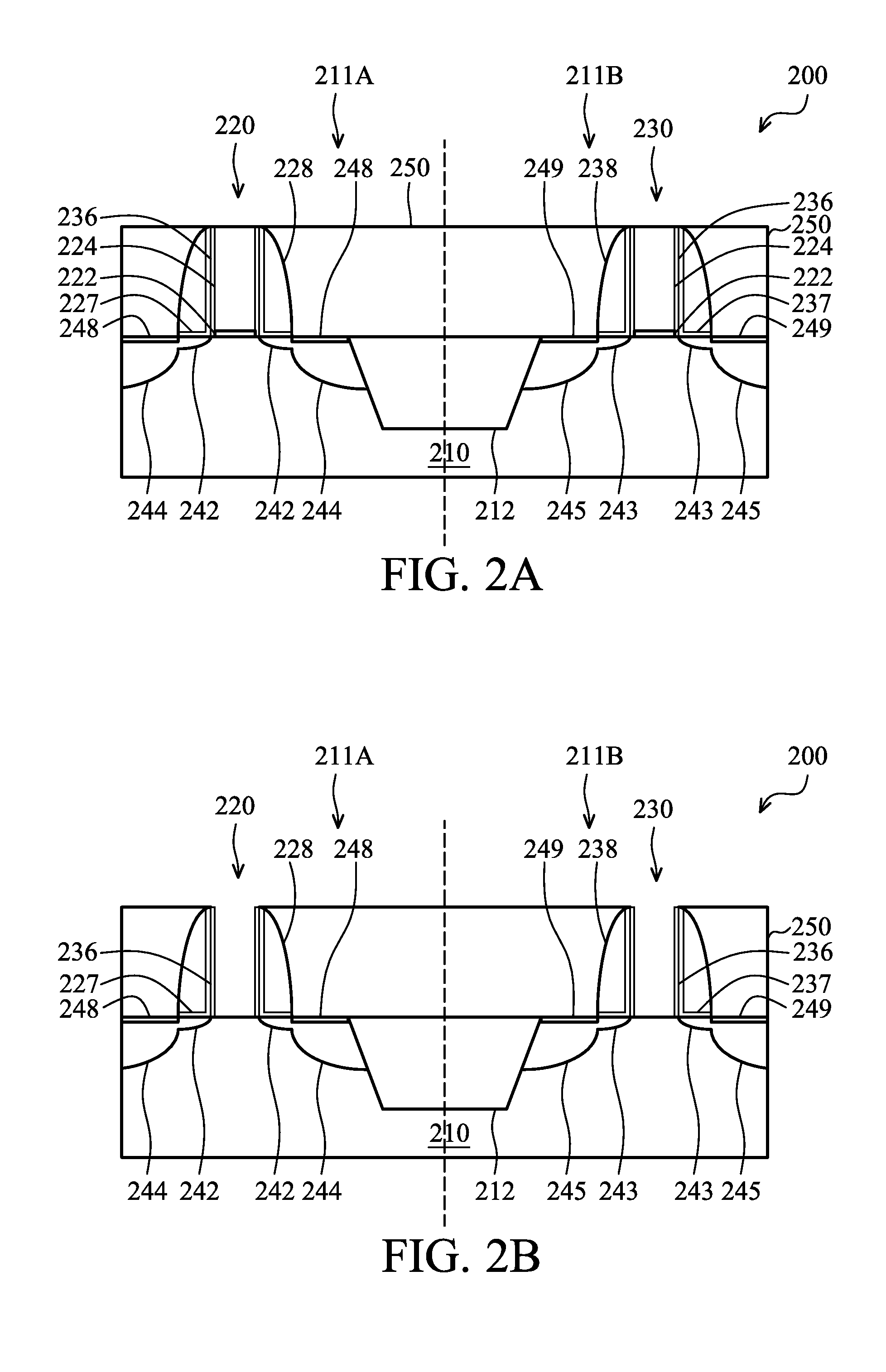
The present disclosure relates generally to methods for manufacturing integrated circuit devices, and more particularly, to gate replacement processes (or methods).
It is understood that the following disclosure provides many different embodiments, or examples, for implementing different features of the invention. Specific examples of components and arrangements are described below to simplify the present disclosure. These are, of course, merely examples and are not intended to be limiting. For example, the formation of a first feature over or on a second feature in the description that follows may include embodiments in which the first and second features are formed in direct contact, and may also include embodiments in which additional features may be formed between the first and second features, such that the first and second features may not be in direct contact. In addition, the present disclosure may repeat reference numerals and / or letters in the various examples. This repetit...
PUM
 Abstract
Description
Claims
Application Information