Multiprocessing circuit with cache circuits that allow writing to not previously loaded cache lines

a multi-processing circuit and cache technology, applied in computing, memory address/allocation/relocation, instruments, etc., can solve the problem of not providing cache consistency for written data, and achieve the effect of increasing the efficiency of a multi-processing system

Inactive Publication Date: 2011-04-07
NXP BV
View PDF8 Cites 5 Cited by
  • Summary
  • Abstract
  • Description
  • Claims
  • Application Information

AI Technical Summary

Benefits of technology

[0012]Among others, it is an object to increase efficiency of a multi-processing system with cache memories.
[0016]In an embodiment memory space is allocated for a cache line in response to a cache miss without loading data from background memory into the cache in response to the cache miss for a write operation. The data from the write operation is then written to the allocated memory space and the flag information is set to indicate selectively that location or those locations as valid where data from the write command is written. Thus, time lost for loading data from background memory is avoided.
[0017]In an embodiment in invalidation signal is generated for a cache miss in the response to a cache miss for a read command when the at least one cache line is in the memory but the flag information indicates the invalid state, by generating an invalidation signal for the cache line. In contrast other cache misses, such as misses due the fact that the cache line is not stored in the cache circuit at all result in read requests. In this way consistent data for read operations is ensured in a simple way.
[0018]In an embodiment a special read request is used in the case of a cache miss for the read command when the at least one cache line is in the memory but the flag information indicates the invalid state. The control circuits of the first and second cache circuit copy background memory data obtained by the special read request selectively only to locations that the flag information indicates not to be in the invalid state. Thus, a need to write back data from the cache line to background memory first is avoided.

Problems solved by technology

Thus, no cache consistency can be provided for written data without having to read cache lines from background memory.

Method used


Image

  • Multiprocessing circuit with cache circuits that allow writing to not previously loaded cache lines
  • Multiprocessing circuit with cache circuits that allow writing to not previously loaded cache lines
  • Multiprocessing circuit with cache circuits that allow writing to not previously loaded cache lines

Examples


Embodiment Construction

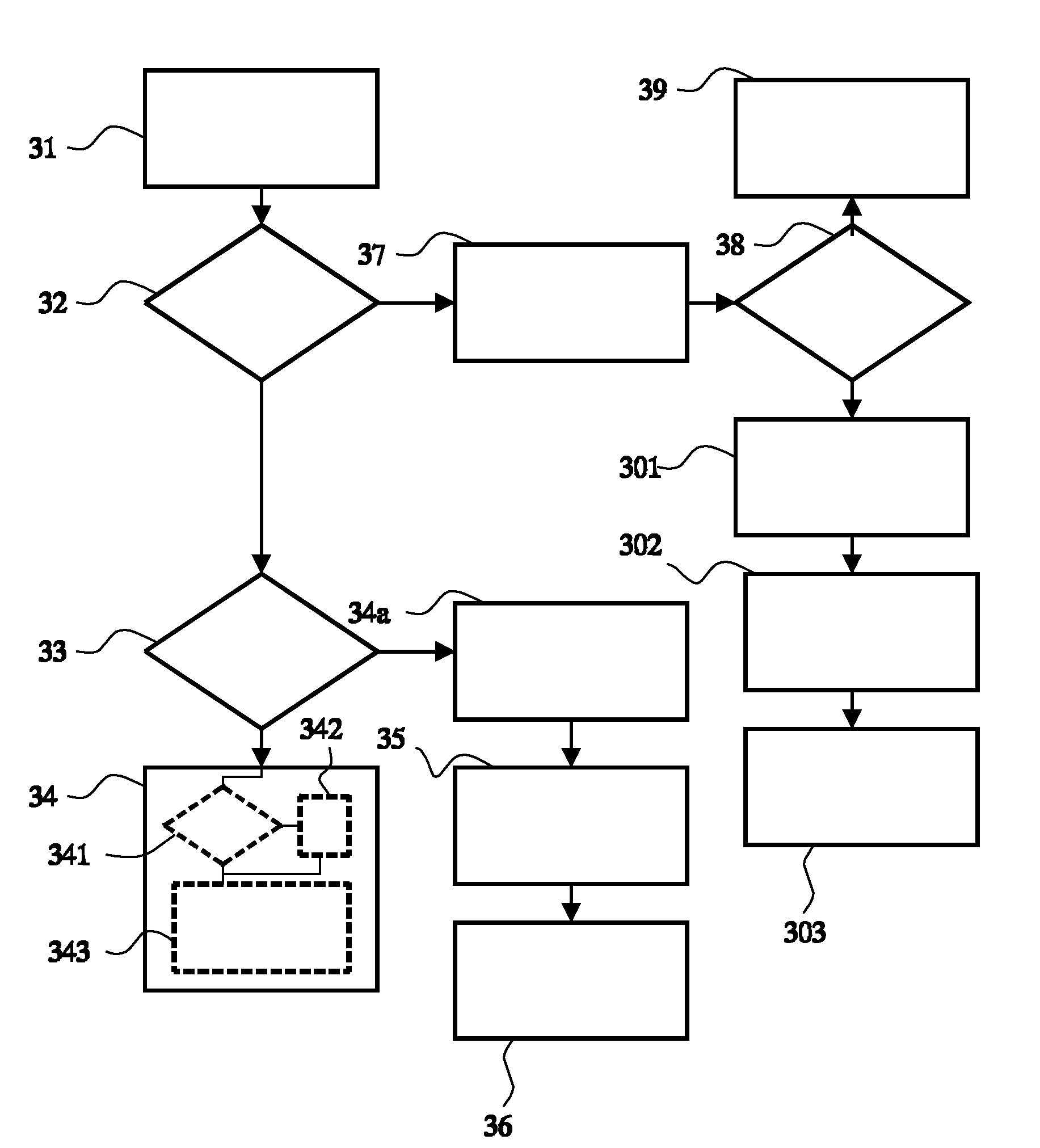
[0023]FIG. 1 shows a multiprocessor system, comprising a main memory 10, a plurality of processor circuits 12 and cache circuits 14, 14′, 14″ coupled between main memory and respective ones of the processor circuits 12. A communication circuit 16 such as a bus may be used to couple the cache circuits 14, 14′, 14″ to main memory 10 and to each other. Processor circuits 12 may comprise programmable circuits, configured to perform tasks by executing programs of instructions. Alternatively, processor circuits 12 may be specifically designed to perform the tasks. Although a simple architecture with one layer of cache circuits between processor circuits 12 and main memory is shown for the sake of simplicity, it should be emphasized that in practice a greater number of layers of caches may be used.

[0024]In operation, when it executes a task, each processor circuit 12 accesses its cache circuit 14, 14′, 14″ by supplying addresses, signaling whether a read or write operation (and optionally ...


PUM


Abstract

Data is processed using a first and second processing circuit (12) coupled to a background memory (10) via a first and second cache circuit (14, 14′) respectively. Each cache circuit (14, 14′) stores cache lines, state information defining states of the stored cache lines, and flag information for respective addressable locations within at least one stored cache line. The cache control circuit of the first cache circuit (14) is configured to selectively set the flag information for part of the addressable locations within the at least one stored cache line to a valid state when the first processing circuit (12) writes data to said part of the locations, without prior loading of the at least one stored cache line from the background memory (10). Data is copied from the at least one cache line into the second cache circuit (14′) from the first cache circuit (14) in combination with the flag information for the locations within the at least one cache line. A cache miss signal is generated both in response to access commands addressing locations in cache lines that are not stored in the cache memory and in response to a read command addressing a location within the at least one cache line that is stored in the memory (140), when the flag information is not set.

Description

FIELD OF THE INVENTION[0001]The invention relates to a multi-processing system and to a method of processing a plurality of tasks.BACKGROUND OF THE INVENTION[0002]It is known to use cache memories between a main memory and respective processor circuits of a multi-processing circuit. The cache memories store copies of data from main memory, which can be addressed by means of main memory addresses. Thus, each processor circuit may access the data in its cache memory without directly accessing the main memory.[0003]In a multi-processing system with a plurality of cache memories that can store copies of the same data, consistency of that data is a problem when the data is modified. If one processor unit modifies the data for a main memory address in its cache memory, loading data from that address main memory may lead to inconsistency, until the modified data has been written back to main memory. Also copies of the previous data for the main memory address in the cache memories of other...

Claims


Application Information

Patent Timeline
Patent Type & Authority Applications(United States)
IPC IPC(8): G06F12/08G06F12/0817
CPCG06F12/0822
Inventor HOOGERBRUGGE, JANTERECHKO, ANDREI SERGEEVICH
Owner NXP BV
Why Eureka
Try Eureka