Semiconductor device and test method thereof

Inactive Publication Date: 2011-04-14
LONGITUDE LICENSING LTD
View PDF11 Cites 49 Cited by
  • Summary
  • Abstract
  • Description
  • Claims
  • Application Information

AI Technical Summary

Benefits of technology

[0013]According to the present invention, because test data are output from different current paths that vary from one memory chip to another, it is possible to output the test data of a plurality of memory chips a

Problems solved by technology

For this reason, it is difficult to greatly increase a memory capacity for each chip.
Therefore there have been a further problem that it is difficult to speed up the front end unit.
However, in the above conventional multichip package or a semiconductor device including a plurality of co

Method used


Image

  • Semiconductor device and test method thereof
  • Semiconductor device and test method thereof
  • Semiconductor device and test method thereof

Examples


Embodiment Construction

[0028]Preferred embodiments of the present invention will be explained below in detail with reference to the accompanying drawings.

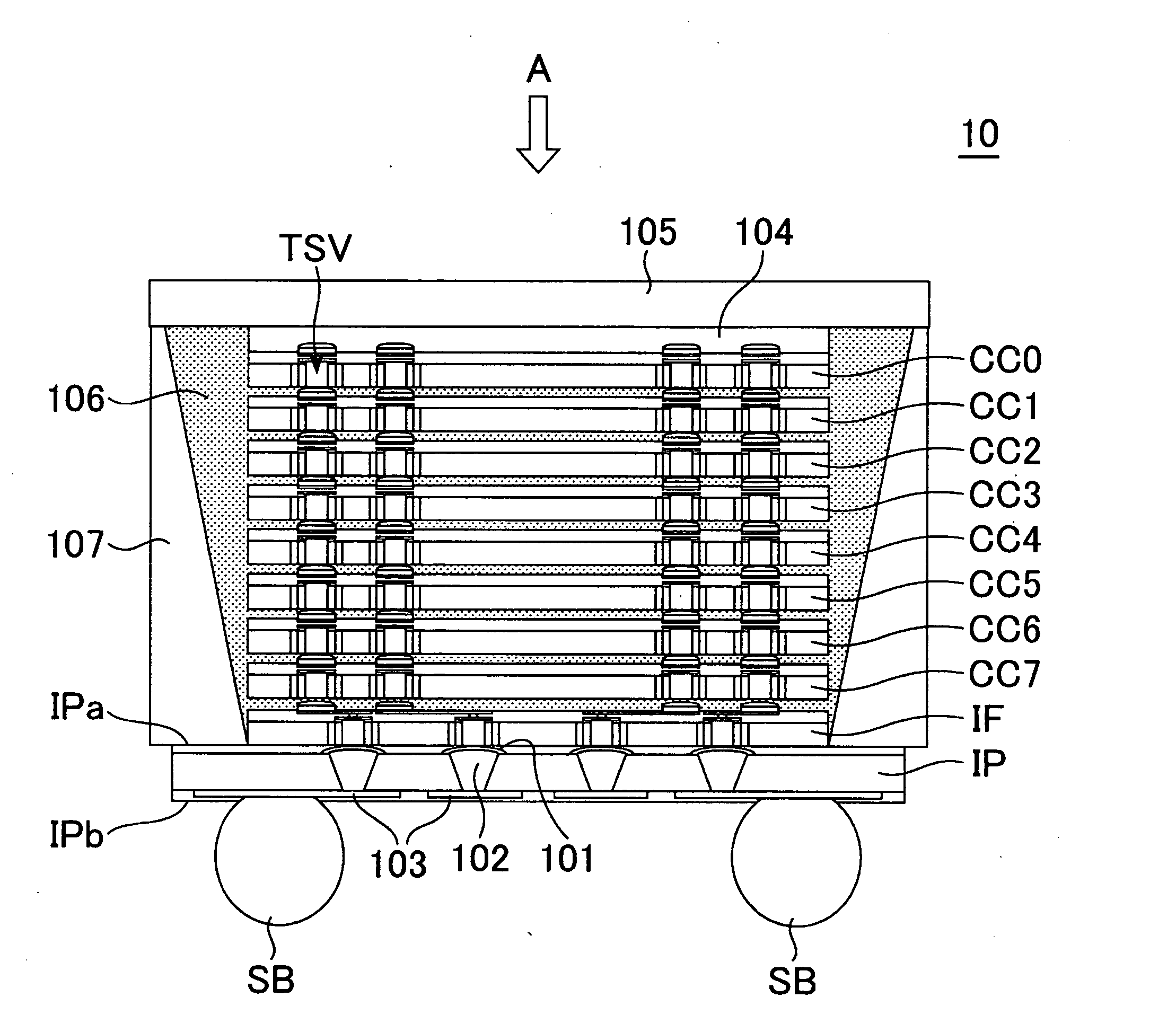
[0029]FIG. 1 is a schematic cross-sectional view provided to explain the structure of a semiconductor memory device 10 according to the preferred embodiment of the present invention.

[0030]As shown in FIG. 1, the semiconductor memory device 10 according to this embodiment has the structure where 8 core chips CC0 to CC7 that have the same function and structure and are manufactured using the same manufacture mask, an interface chip IF that is manufactured using a manufacture mask different from that of the core chips and an interposer IP are laminated. The core chips CC0 to CC7 and the interface chip IF are semiconductor chips using a silicon substrate and are electrically connected to adjacent chips in a vertical direction through plural through silicon vias TSV penetrating the silicon substrate. Meanwhile, the interposer IP is a circuit board that is mad...


PUM


Abstract

A semiconductor device includes a plurality of memory chips arranged in a layered manner, each including a substrate and a memory cell array, and a plurality of current paths provided while penetrating through the memory chips. Each of the memory chips includes a test circuit that reads test data from a corresponding one of the memory cell array and outputs a layer test result signal responding to the test data to a different current path for each of the memory chips.

Description

BACKGROUND OF THE INVENTION[0001]1. Field of the Invention[0002]The present invention relates to a semiconductor device and a test method thereof, and more particularly relates to a semiconductor device that includes a plurality of core chips and an interface chip for controlling the core chips and a test method thereof.[0003]2. Description of the Related Art[0004]A memory capacity that is required in a semiconductor memory device such as a DRAM (Dynamic Random Access Memory) are increasing every year. To satisfy this requirement by increasing a memory capacity of each memory chip prevents to secure a yield rate because it requires finer processing than so far. Therefore, in recent years, a memory device that is called a multi-chip package where plural memory chips are laminated is suggested to satisfy the required memory capacity (see Japanese Patent Application Laid-Open (JP-A) No. 2002-305283). However, since the memory chip used in the multi-chip package is a common memory chip ...

Claims


Application Information

Patent Timeline
IPC IPC(8): G01R31/26
CPCG11C5/02G11C5/04G11C29/1201G11C29/48H01L2924/01055H01L2924/15311H01L2924/01019H01L2924/01037H01L2224/16145
Inventor NISHIOKA, NAOHISA
Owner LONGITUDE LICENSING LTD
Why Eureka
Try Eureka