Intrusion protection using stress changes

a technology of intrusion protection and stress change, applied in the direction of mechanical actuation of burglar alarms, acceleration measurement using interia forces, instruments, etc., can solve the problems of local change in stress on the substrate and strain change on the substra

Active Publication Date: 2011-04-21
NXP BV
View PDF3 Cites 26 Cited by
  • Summary
  • Abstract
  • Description
  • Claims
  • Application Information

AI Technical Summary

Benefits of technology

[0006]It is an object of the invention to provide an integrated circuit with an alte

Problems solved by technology

Tampering with the integrated circuit implies a partial removal of the first strained encapsulation layer which in

Method used


Image

  • Intrusion protection using stress changes
  • Intrusion protection using stress changes
  • Intrusion protection using stress changes

Examples


Embodiment Construction

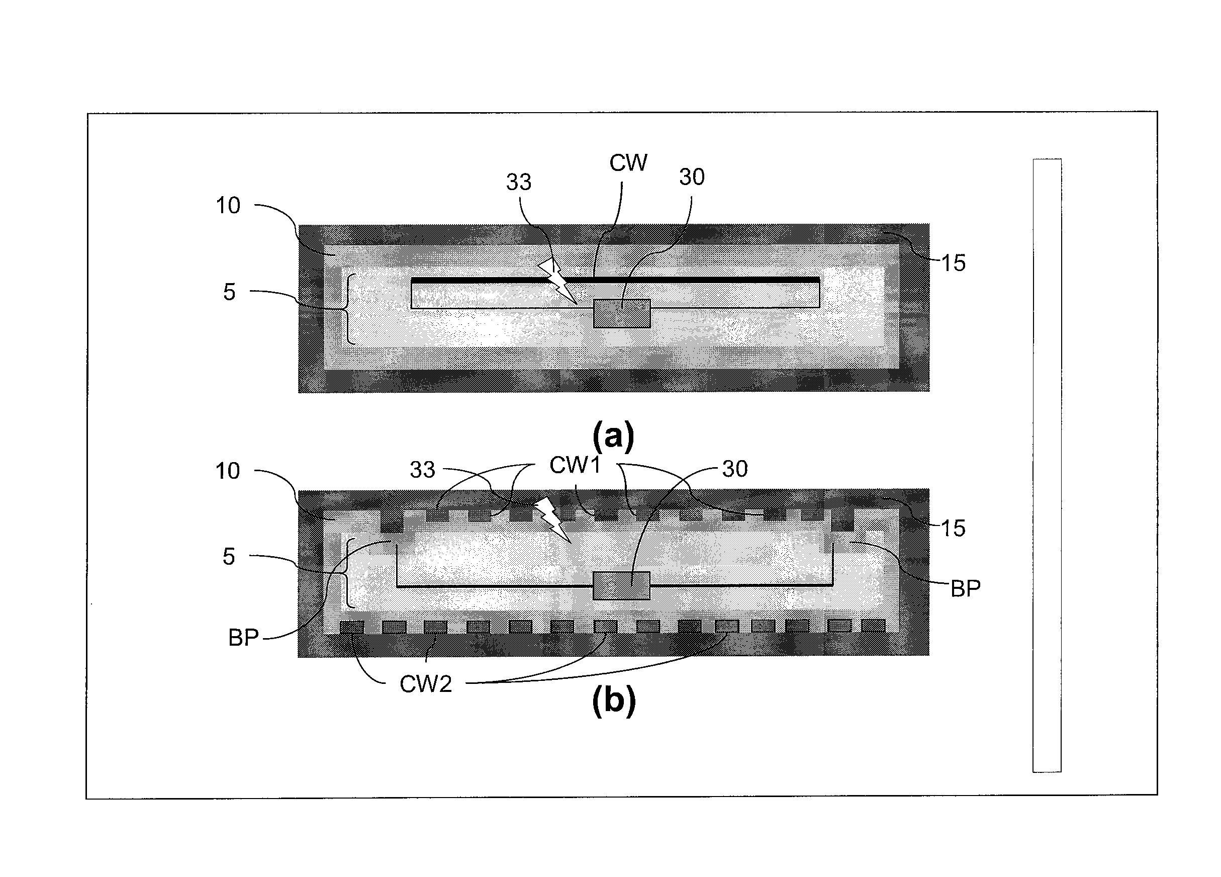
[0041]The invention provides for a new tamper protection technique against invasive attack techniques, which helps to stay ahead of hackers. Hackers are known for keeping on improving their attack techniques for retrieving secret data from integrated circuits. Especially integrated circuits having memory elements, such as non-volatile memories (ROM, EPROM, EEPROM, FLASH, MRAM, etc) are of interest for hackers as these often contain secret keys for encryption purposes or other data which needs protection. The tamper protection technique provided by the invention may be advantageously combined with known tamper protection techniques from the prior art. Such combination may result in even higher protection levels. Remarks to this extent are only made in as far as such combination is not self-explaining.

[0042]In order to facilitate the discussion of the detailed embodiments a few expressions are defined hereinafter.

[0043]Throughout this description the term “encapsulation layer” refers ...


PUM


Abstract

The invention relates to a integrated circuit comprising an electronic circuit integrated on a substrate (5), and further comprising protections means for protection of the electronic circuit (25). The protection means comprise: i) a first strained encapsulation layer (10) being provided on a first side of the substrate (5), wherein the first strained encapsulation layer (10) has a strain (S1) in a direction parallel to the substrate (5), and ii) disabling means (20) arranged for at least partially disabling the electronic circuit (25) under control of a strain change in the substrate (5). The invention further relates to a method of manufacturing such integrated circuit, and to a system comprising such integrated circuit. Such system is selected from a group comprising: a bank-card, a smart-card, a contact-less card and an RFID. All embodiments of the integrated circuit in accordance with the invention provide essentially an alternative tamper protection to the data stored or present in the electronic circuit therein. A first main group of embodiments concerns an integrated circuit wherein tamper protection is obtained by detecting a strain change during tampering and subsequently disabling the electronic circuit. A second main group of embodiments concerns an integrated circuit wherein tamper protection is obtained by designing a stack of strained encapsulation layers, such that tampering causes releasing of strain and thereby mechanical disintegrate (break, delaminate, etc) of the integrated circuit, and thus disabling the electronic circuit.

Description

FIELD OF THE INVENTION[0001]The invention relates to an integrated circuit comprising an electronic circuit integrated on a substrate, and further comprising protections means for protection of the electronic circuit. The invention further relates to a method of manufacturing such integrated circuit. The invention also relates to a system comprising such integrated circuit.BACKGROUND OF THE INVENTION[0002]Nowadays, much (personal) data is stored on memory modules embedded in systems, such as smartcards for pay-TV or electronic purses. In order to protect data, security should be as high as possible. Typically, the data is protected from external read-out with a secure key. Once the key is known, the data can be read out. The external read-out of data by decryption of the data is known as a non-invasive attack.[0003]In invasive attacks the chip is de-packaged, where the goal is direct read-out of the data in the memory or disabling the key by UV radiation. Both approaches require rem...

Claims


Application Information

Patent Timeline
IPC IPC(8): H01L29/84G06K19/073H01L21/56G06F21/87
CPCG06F21/87H01L23/576H01L2924/0002H01L2924/00
Inventor HOOFMAN, ROMANOPIJNENBURG, REMCO HENRICUS WILHELMUSPONOMAREV, YOURI VICTOROVITCH
Owner NXP BV
Why Eureka
Try Eureka