Thin film surface mount components

a surface mount and component technology, applied in the direction of fixed capacitor details, electric apparatus casings/cabinets/drawers, instruments, etc., can solve the problems of limiting the miniaturization potential of components, significant amount of component real estate, undesirable effects on circuit performance, etc., to achieve enhanced circuit functionality and reduce termination costs

Active Publication Date: 2011-04-21
KYOCERA AVX COMPONENTS CORP
View PDF36 Cites 63 Cited by
  • Summary
  • Abstract
  • Description
  • Claims
  • Application Information

AI Technical Summary

Benefits of technology

[0012]In some exemplary configurations, a thin film component is provided with plated termination features that may be formed using batch plating processes, thus substantially lowering termination costs associated with such devices.
[0013]In some exemplary configurations, a thin film component is provided with one or more multilayer cover substrates that includes enhanced circuit functionality, in the form of additional circuitry, capacitive elements, protective functionality or other features.

Problems solved by technology

Relatively larger termination features can require valuable real estate within an electronic component, thus limiting potential component miniaturization.
Larger termination features may also introduce higher levels of equivalent series inductance (ESL), which can yield undesirable effects in circuit performance, especially at high operating frequencies.
Such techniques often require a significant amount of component real estate on the active component surface(s) for the formation of solder balls or lands.
In addition, components having such termination arrangements are often limited to mounting on only one side of a component.
The BGA technique illustrated in FIG. 15 as well as other known techniques such as LGA and wire bonding not only often require a significant amount of component real estate on the active component surface(s) for the formation of solder balls or lands, but also typically add substantial cost to the finished component.
In addition, components having such termination arrangements are often limited to mounting on only one side of a component.
Such thin film circuits remain without additional possible circuit functionality and / or structural protection provided on top of the thin film circuit(s).
While various implementations of passive electronic components and associated features have been developed, no design has emerged that generally encompasses all of the desired characteristics as hereafter presented in accordance with the subject technology.

Method used


Image

  • Thin film surface mount components
  • Thin film surface mount components
  • Thin film surface mount components

Examples


embodiment 1300

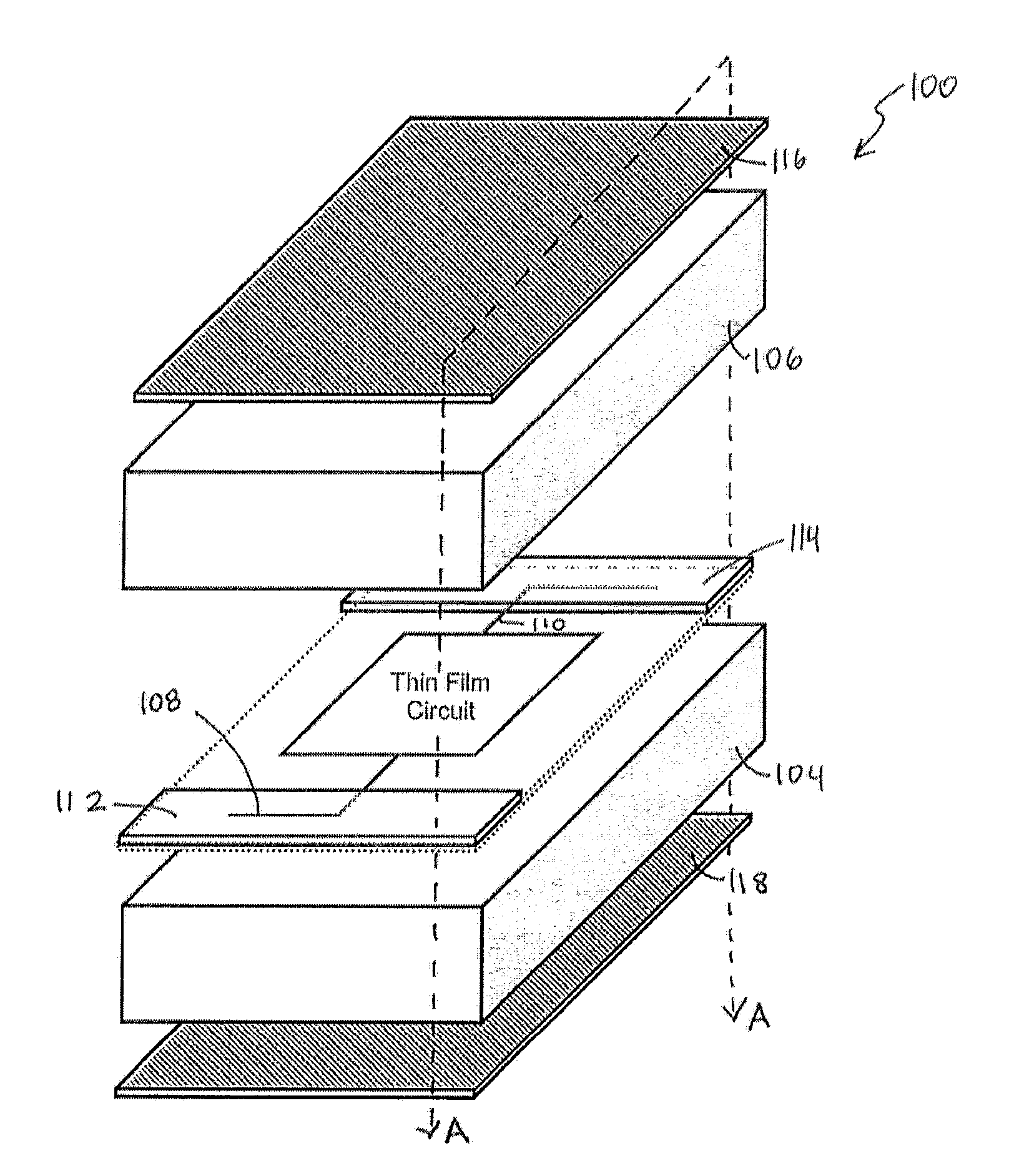
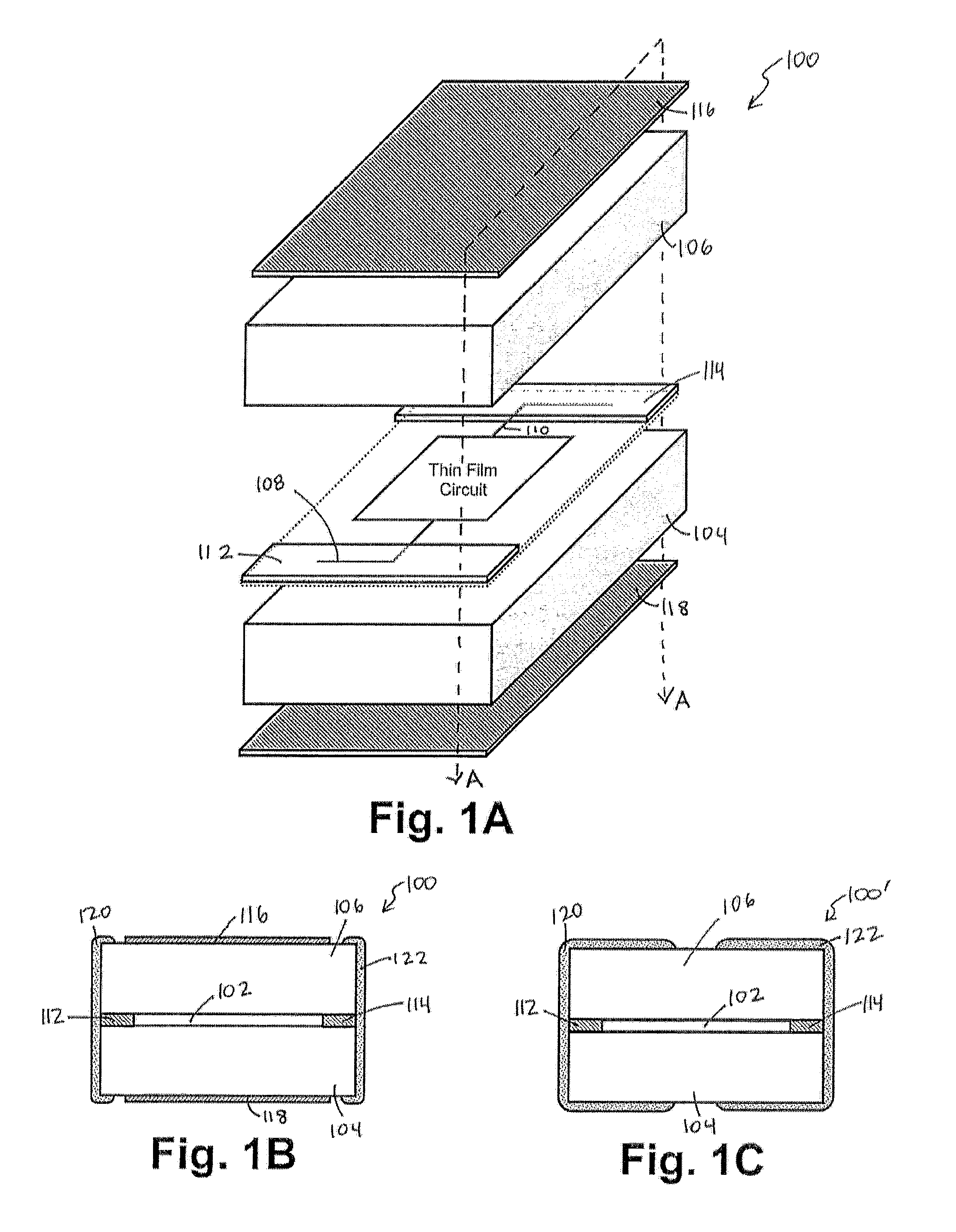
[0139]Referring now to FIG. 18, an exemplary thin film surface mount component embodiment 1300 includes a thin film circuit 1301 formed on a surface of base substrate 1302. At least first and second conductive pads 1303 and 1305 are also formed on the upper surface of base substrate 1302 to form at least first and second electrical connections to thin film circuit 1301. A layer of adhesive 1304 is formed on top of the thin film circuit 1301 and first and second conductive pads 1303, 1305. In alternative embodiments, adhesive layer 1304 is formed only over the thin film circuit 1301 and not over the first and second conductive pads 1303, 1305. On top of adhesive layer 1304 is provided a multilayer cover substrate 1306.

[0140]In component 1300, cover substrate 1306 includes layers of dielectric material and alternately interleaved active electrode layers 1312, 1314 that overlap in adjacent electrode planes to form opposing electrodes in respective parallel plate capacitors. A plurality...

embodiment 1400

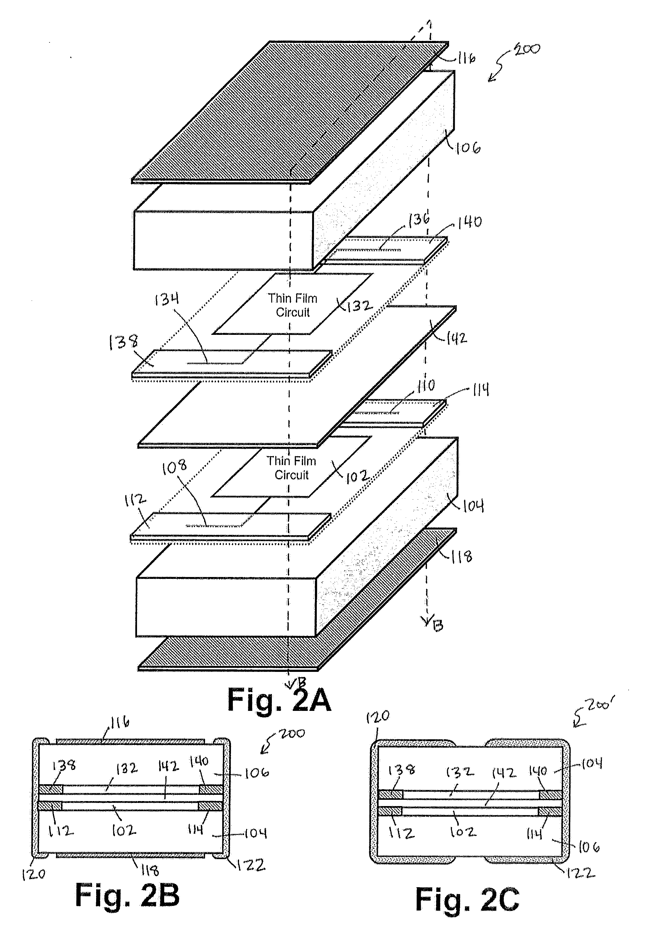
[0141]Referring now to FIG. 19, an exemplary thin film surface mount component embodiment 1400 includes a thin film circuit 1401 formed on a surface of base substrate 1402. At least first and second conductive pads 1403 and 1405 are also formed on the upper surface of base substrate 1402 to form at least first and second electrical connections to thin film circuit 1401. A layer of adhesive 1404 is formed on top of the thin film circuit 1401 and first and second conductive pads 1403, 1405. In alternative embodiments, adhesive layer 1404 is formed only over the thin film circuit 1401 and not over the first and second conductive pads 1403, 1405. On top of adhesive layer 1404 is provided a multilayer cover substrate 1406.

[0142]In component 1400, cover substrate 1406 includes layers of dielectric material and alternately interleaved active electrode layers 1412, 1414 that overlap in adjacent planes electrode to form opposing electrodes in respective parallel plate capacitors. The respect...


PUM

PropertyMeasurementUnit
thicknessaaaaaaaaaa
thicknessaaaaaaaaaa
thicknessaaaaaaaaaa

Abstract

Surface mount components and related methods of manufacture involve one or more thin film circuits provided between first and second insulating substrates. The thin film circuits may include one or more passive components, including resistors, capacitors, inductors, arrays of one or more passive components, networks or filters of multiple passive components. Such thin film circuit(s) can be sandwiched between first and second insulating substrates with internal conductive pads being exposed between the substrates on end and / or side surfaces of the surface mount component. The exposed conductive pads are then electrically connected to external terminations. The external terminations may include a variety of different materials, including at least one layer of conductive polymer and may be formed as termination stripes, end caps or the like. Optional shield layers may also be provided on top and / or bottom device surfaces to protect the surface mount components from signal interference. For embodiments where one or more thin film circuits are provided between insulating base and cover substrates, such thin film circuit(s) can be formed with conductive pads that extend to and are initially exposed along one or more surfaces of the resultant component. The cover substrate is formed with a plurality of conductive elements (e.g., internal active electrodes, internal anchor electrodes and / or external anchor electrodes) that are designed to generally align with the conductive pads formed on the base substrate such that conductive element portions are exposed in groups along one or more peripheral surfaces of a device. External plated terminations are then formed directly to the exposed portions of the conductive elements.

Description

PRIORITY CLAIM[0001]This application claims the benefit of previously filed U.S. Provisional Patent Application entitled “THIN FILM SURFACE MOUNT COMPONENTS,” assigned U.S. Ser. No. 61 / 252,340, filed Oct. 16, 2009, and claims the benefit of previously filed U.S. Provisional Patent Application entitled “THIN-FILM SURFACE MOUNT COMPONENTS WITH PLATED TERMINATIONS,” assigned U.S. Ser. No. 61 / 252,335, filed Oct. 16, 2009, and both of which are fully incorporated herein by reference for all purposes.FIELD OF THE INVENTION[0002]The present subject matter generally relates to small electronic components adapted for mounting on a circuit board or other surface-mountable location. More particularly, the present subject matter relates to surface mount components having one or more thin film circuits of passive components for use in a variety of applications, as well as related methods for producing such devices.BACKGROUND OF THE INVENTION[0003]For some time, the design of various electronic c...

Claims


Application Information

Patent Timeline
Patent Type & Authority Applications(United States)
IPC IPC(8): H05K7/00H05K3/00
CPCH01C1/148H01C7/006H01F5/003H01G4/224H01G4/248Y10T29/49124H03H7/0115H03H2001/0085H01L2924/0002H01G4/33H01L2924/00H01C17/00H01F41/00H01F27/2804H01F2027/2809H03H7/17H05K1/111H05K1/186H05K3/4611H05K3/467H05K3/4697
Inventor KORONY, GHEORGHERITTER, ANDREW P.
Owner KYOCERA AVX COMPONENTS CORP
Why Eureka
Try Eureka