Method of Embedding Material In A Glass Substrate

a technology of glass substrate and material, applied in the direction of machines/engines, positive displacement liquid engines, transportation and packaging, etc., can solve the problems of inability to achieve sufficient spatial resolution with sufficient repeatability, traditional glass molding techniques are not considered and the surface wettability of the patterned surface is increased. , the effect of increasing the surface wettability

Active Publication Date: 2011-04-21
RGT UNIV OF MICHIGAN
View PDF24 Cites 19 Cited by
  • Summary
  • Abstract
  • Description
  • Claims
  • Application Information

AI Technical Summary

Benefits of technology

[0010]The step of increasing the surface wettability of the patterned surface of the mold substrate relative to the glass composition results in more complete bonding between the solidified glass layer and the patterned surface of the mold substrate. In particular, it is notable that, even by creating a vacuum in the recesses as is practiced in known processes of structuring wafers comprising glass and silicon regions, complete filling of the recesses (especially corners thereof) with the glass composition during the flowing step remains a challenge and it has been found that gaps in bonding are present between the resolidified glass region and side walls of the mold substrate in the recesses. As a result of incomplete filling of the recesses with the glass, substrates that comprise glass and material embedded therein through existing processes generally cannot be thinned below a threshold thickness without fracturing due to insufficient bonding between the resolidified glass regions and the side walls of the mold substrate in the recesses. Furthermore, it is difficult to adequately flow the glass into recesses having a width of less than 100 μm. By increasing the surface wettability of the patterned surface of the mold substrate relative to the glass composition, the flow of the glass composition over the patterned surface is promoted, which results in more complete bonding, leads to the ability to thin the resulting glass substrates the electrically-conductive material embedded therein to thicknesses that have not been achievable to date without fracturing, and enables adequate filling of recesses having widths of less than 100 μm.

Problems solved by technology

However, there is often a need to convey electrical signals between electrical components that are separated by insulative components.
However, formation of electronic feedthroughs or vias in glass is particularly problematic in the field of electronic microsystems and has often led to a preference for polymeric materials for use in the insulative components.
Due to the extremely small dimensions of the holes, traditional glass molding techniques are not considered.
The aforementioned processes used to generate holes in the glass suffer from drawbacks such as an inability to achieve sufficient spatial resolution with sufficient repeatability, propensity to damage the glass or alter the surface thereof in an undesirable manner, limitations as to the size of holes that can be generated, and / or limitation to batch mode processing.
However, wafers that comprise glass and silicon regions formed through the process as described above are extremely fragile and generally cannot be thinned below the thickness of 0.1 mm without fracturing due to insufficient adhesion between the glass and silicon regions.
While portions of the wafers may be salvaged, fracturing is undesirable and complicates additional processing steps.
Furthermore, it is difficult to obtain adequate flow of the glass into recesses having a width of less than 100 μm.

Method used


Image

  • Method of Embedding Material In A Glass Substrate
  • Method of Embedding Material In A Glass Substrate
  • Method of Embedding Material In A Glass Substrate

Examples


Embodiment Construction

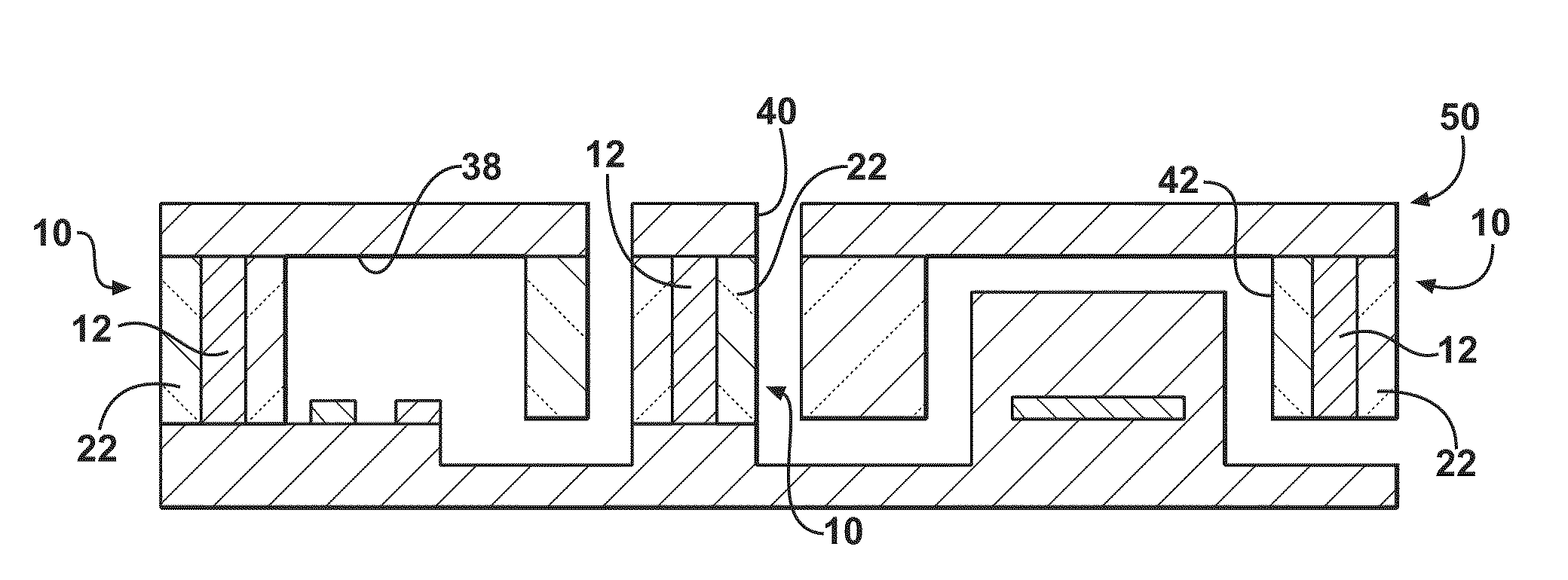
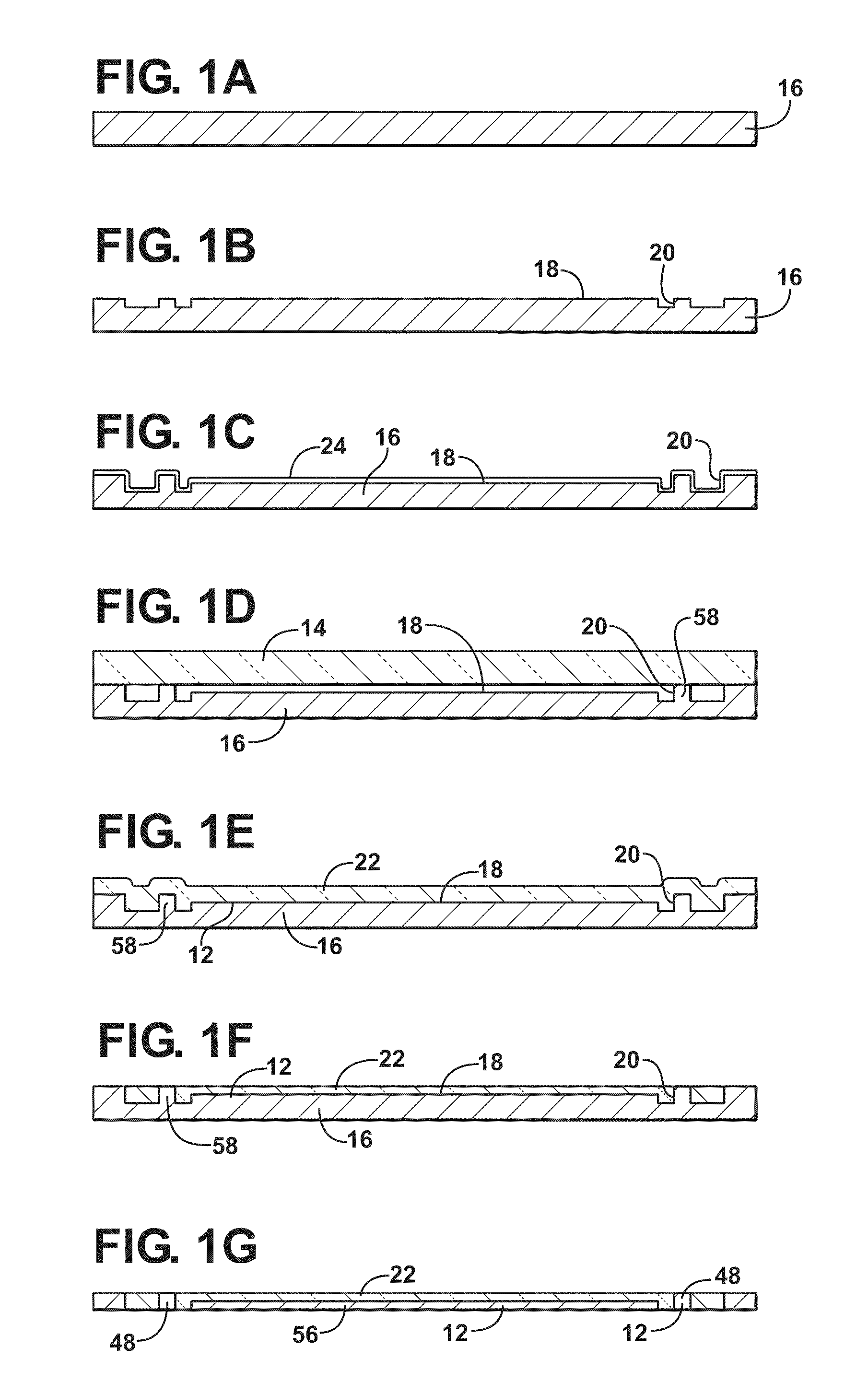
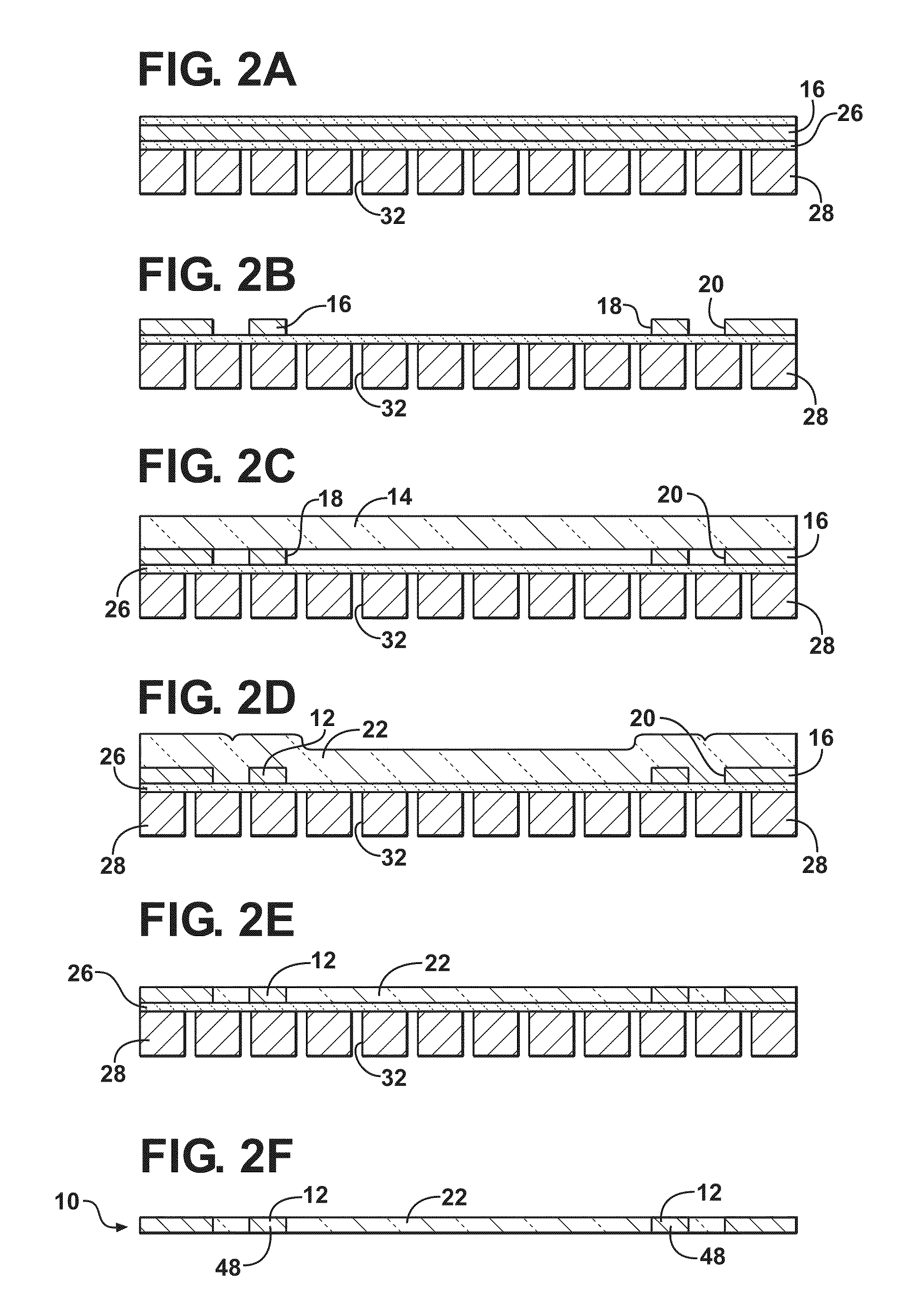
[0022]Referring to the Figures, where like numerals indicate like or corresponding parts through the several views, a method of embedding material 12 in a glass substrate 10 is provided herein and is shown schematically in FIGS. 1 and 2. The glass substrates 10 formed in accordance with the method of the instant invention have wide-ranging uses as described in further detail below, especially for purposes of solving problems associated with forming through-glass vias 48 and other electrically-conductive elements embedded in glass for use in electronic microsystem applications such as implantable microsystems, where biocompatibility, size, and extremely low power consumption are design considerations. The method of the instant invention avoids many problems associated with conventional techniques for embedding material in glass, and further alleviates conditions that limit minimum thicknesses that can be achieved for glass substrates 10 including material 12 embedded therein that are...


PUM

PropertyMeasurementUnit
depthaaaaaaaaaa
total thicknessaaaaaaaaaa
thicknessaaaaaaaaaa

Abstract

A method of embedding material in a glass substrate is provided. The method includes providing a glass composition and a mold substrate having a patterned surface defining a recess therein. The mold substrate is formed from a material having a higher reflow temperature than the glass composition. A surface wettability of the patterned surface is increased relative to the glass composition. At least a portion of the glass composition is flowed into the recess defined by the patterned surface of the mold substrate, followed by solidifying the glass composition to form a solidified glass layer. Material is removed from the solidified glass layer until a portion of the underlying patterned surface of the mold substrate is exposed with at least a portion of the mold substrate embedded in the solidified glass layer to thereby form the glass substrate having the material embedded therein.

Description

BACKGROUND OF THE INVENTION[0001]1. Field of the Invention[0002]The instant invention generally relates to a method of embedding material in a glass substrate. More specifically, the instant invention relates to a method of flowing a glass composition into a recess in a patterned surface of a mold substrate formed from the material to form a glass substrate, with the resulting glass substrate having the material of the mold substrate embedded therein.[0003]2. Description of the Related Art[0004]The field of electronic microsystems covers a broad array of technologies that benefit from functionality of electronic devices but in which minimal size is desired. For example, implantable devices, batteries, integrated circuits, microfluidic circuits and associated devices such as pumps and valves represent a few technologies that benefit from advances in the field of electronic microsystems. There is a constant drive to make advances in the field of electronic microsystems that enables fu...

Claims


Application Information

Patent Timeline
Patent Type & Authority Applications(United States)
IPC IPC(8): C03C14/00C03C19/00B32B3/00
CPCB81B2201/036B81B2201/058Y10T428/24479C03C19/00F04B19/006B81C1/00095
Inventor HAQUE, RAZI-ULWISE, KENSALL
Owner RGT UNIV OF MICHIGAN
Why Eureka
Try Eureka