
Eureka
For R&D, Eureka makes reading and utilizing patents & technical documents easy.
Eureka AIR
Designed for self-driven R&D workflows. Generate viable solutions, solve complex R&D challenges, empower your innovation with AI.

Eureka Materials
Designed for material experts only. Revolutionize your material R&D, from search, analyze, to developing new materials.

TechResearch
Generate reliable direction feasibility study reports for your R&D in just a few steps.

TechSeek
Discover and master advanced knowledge NOW. Basics, ideas, possibilities, all at once.

TechMind
As an expert in R&D Theories, TechMind can generates customized viable solutions instantly.

TechRisk
Analyze your overall solution with one click, know your potential R&D risks in advance.

TechMonitor
Get weekly tech updates, stay abreast of the latest tech innovations and key insights.
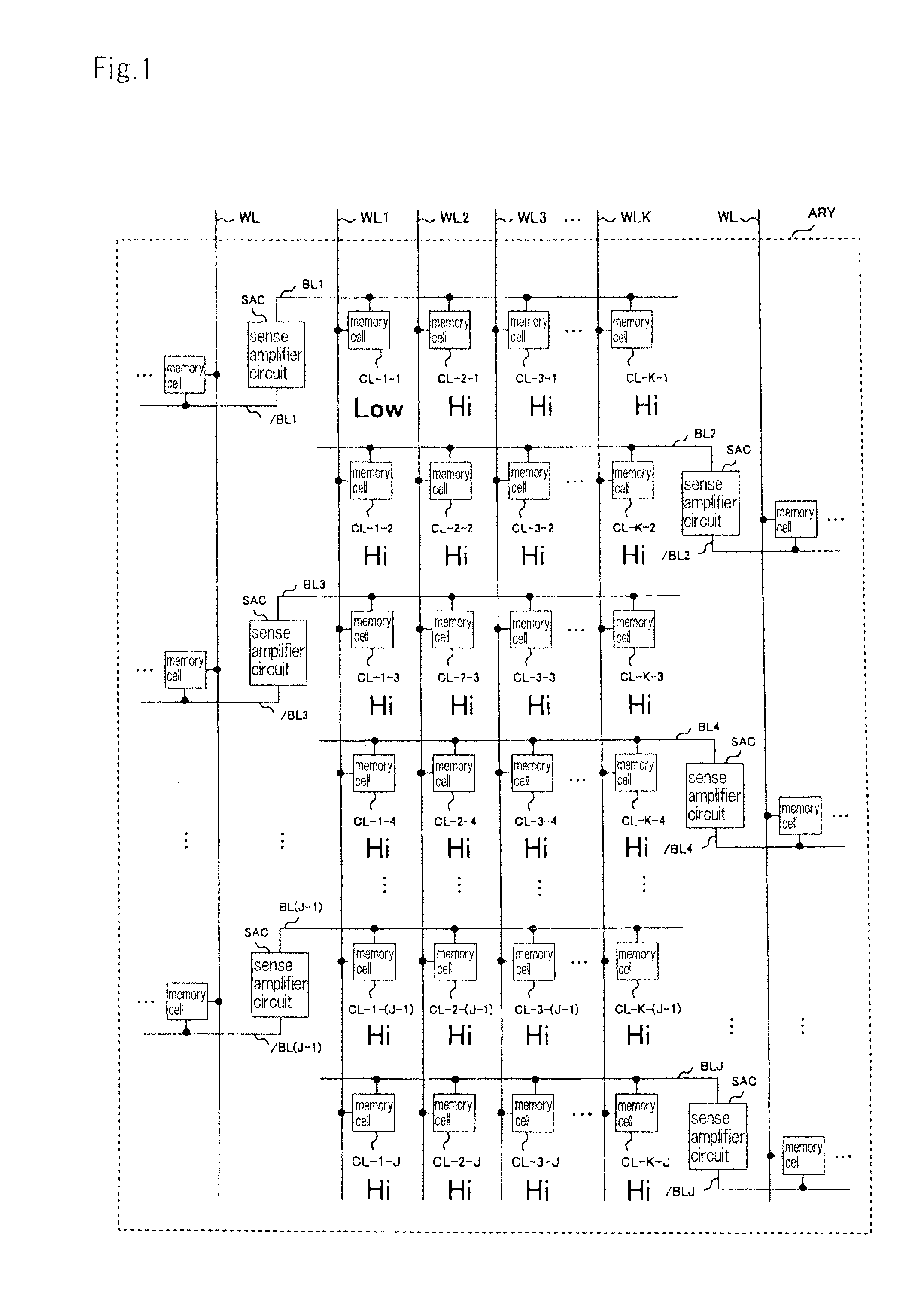
Sense amplifier circuit to enable speeding-up of readout of information from memory cells
- Summary
- Abstract
- Description
- Claims
- Application Information
AI Technical Summary
Benefits of technology
Problems solved by technology
Method used
Image

Examples
first embodiment
[0041
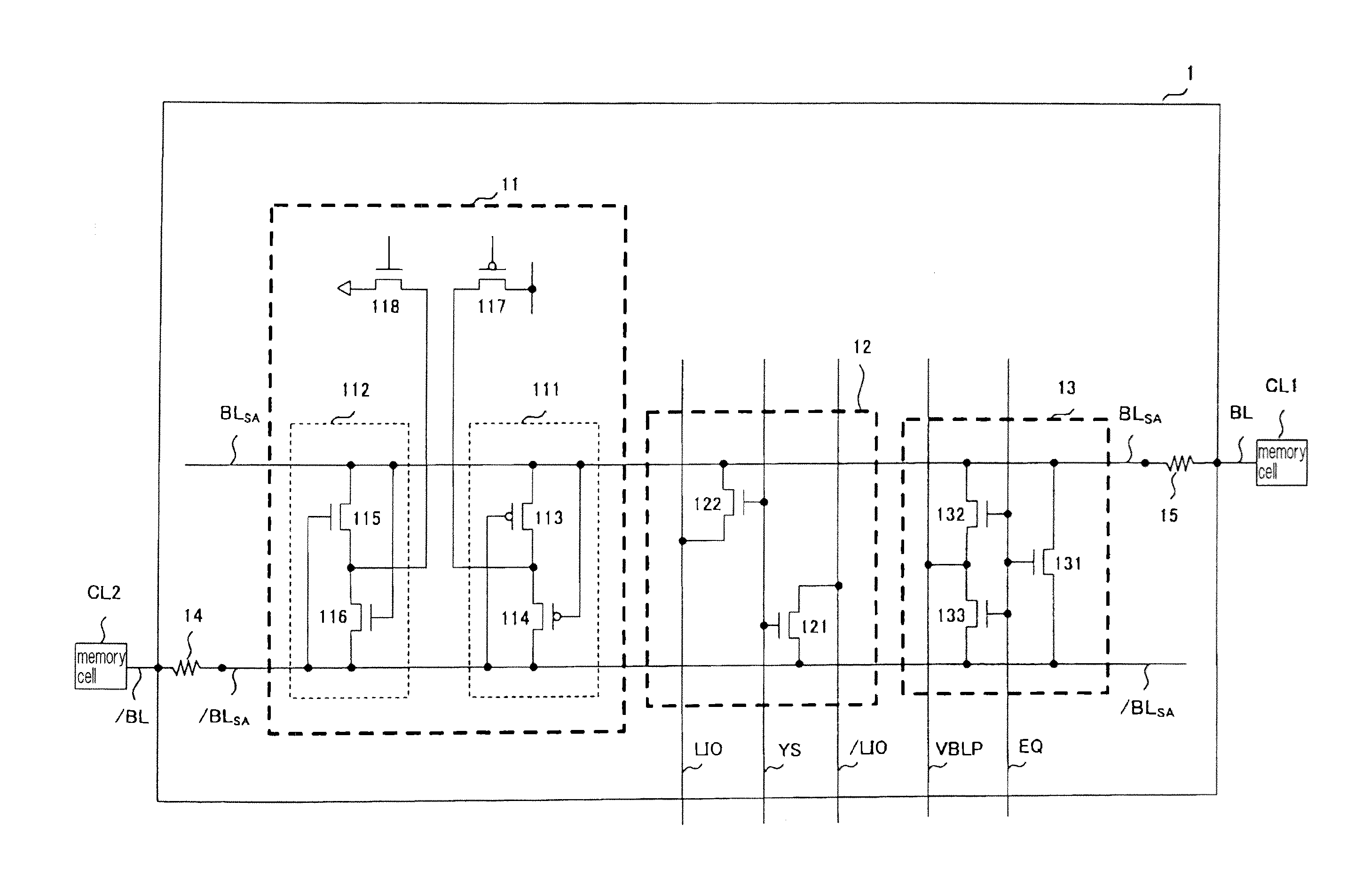
[0042]A semiconductor device according to a first embodiment of the present invention will be described. The configuration of sense amplifier circuit 1 provided in the semiconductor device in the present embodiment will first be described in detail with reference to FIG. 7.
[0043]As shown in FIG. 7, amplification section 11, Y switch 12 and equalizer 13 are provided in sense amplifier circuit 1. Internal bit line BLSA provided in sense amplifier circuit 1 is connected to bit line BL through second resistance section 15. Also, internal inverted bit line / BLSA provided in sense amplifier circuit 1 is connected to inverted bit line / BL through first resistance section 14.
[0044]In the first embodiment, first resistance section 14 and second resistance section 15 are resistance elements having a predetermined resistance component respectively.
[0045]Bit line BL is connected to memory cell CL1, while inverted bit line / BL is connected to memory cell CL2.
[0046]Sense amplifier circuit 1 ...
second embodiment
[0084
[0085]A semiconductor device in a second embodiment of the present invention will be described.
[0086]In the semiconductor device in the first embodiment, first resistance section 14, which is a resistance element, is provided between inverted bit line / BL and sense amplifier circuit 1, and second resistance section 15, which is another resistance element, is provided between bit line BL and sense amplifier circuit 1, as shown in FIG. 7.
[0087]In the case where resistance elements are added as components of first resistance section 14 and second resistance section 15, however, the memory cell area of the DRAM is increased.
[0088]In the second embodiment, a reduction in the speed at which information from memory cells is read out is avoided while avoiding an increase in memory cell area.
[0089]In the semiconductor device in the second embodiment, sense amplifier circuit 1A is provided in place of sense amplifier circuit 1 shown in FIG. 7. The configuration of sense amplifier circuit...
third embodiment
[0119
[0120]A semiconductor device in a third embodiment of the present invention will be described.
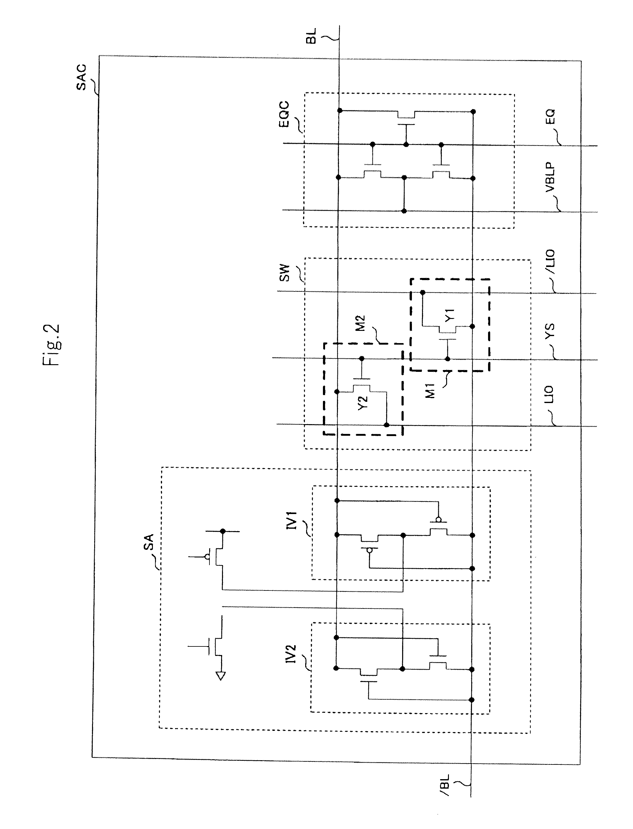
[0121]In the semiconductor device in the third embodiment, sense amplifier circuit 1B is provided in place of sense amplifier circuit 1 shown in FIG. 7. The configuration of this sense amplifier circuit 1B will be described in detail with reference to FIG. 13.
[0122]As shown in FIG. 13, sense amplifier circuit 1B differs from sense amplifier circuit 1 in the first embodiment in that first transistor 141 is provided in place of first resistance section 14 shown in FIG. 7 and second transistor 151 is provided in place of second resistance section 15 shown in FIG. 7.
[0123]In the third embodiment, an “on-resistance” which is the resistance value between the drain electrode and the source electrode of first transistor 141 is used as a resistance component of first resistance section 14 shown in FIG. 7. Also, the on-resistance of second resistance section 15 is used as a resistance component ...
PUM
 Abstract
Description
Claims
Application Information
 - R&D Engineer
- R&D Manager
- IP Professional
- Industry Leading Data Capabilities
- Powerful AI technology
- Patent DNA Extraction
Browse by: Latest US Patents, China's latest patents, Technical Efficacy Thesaurus, Application Domain, Technology Topic, Popular Technical Reports.
© 2024 PatSnap. All rights reserved.Legal|Privacy policy|Modern Slavery Act Transparency Statement|Sitemap|About US| Contact US: help@patsnap.com