

Method of forming a liquid crystal layer, method of manufacturing a liquid crystal display panel using the method, and liquid crystal material used in the method
a technology of liquid crystal display panel and liquid crystal layer, which is applied in the direction of coating, chemistry apparatus and processes, and lamination ancillary operations. it can solve the problems of complex process for disposing liquid crystal material, large droplet of liquid crystal material on a substrate, and uneven droplet of liquid crystal material. it is easy to control and the position error of the droplet is reduced
- Summary
- Abstract
- Description
- Claims
- Application Information
AI Technical Summary
Benefits of technology
Problems solved by technology
Method used
Image

Examples
Embodiment Construction
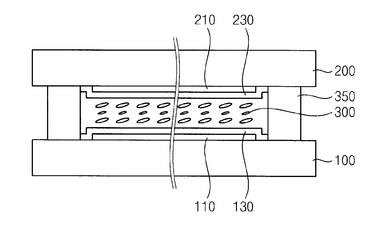
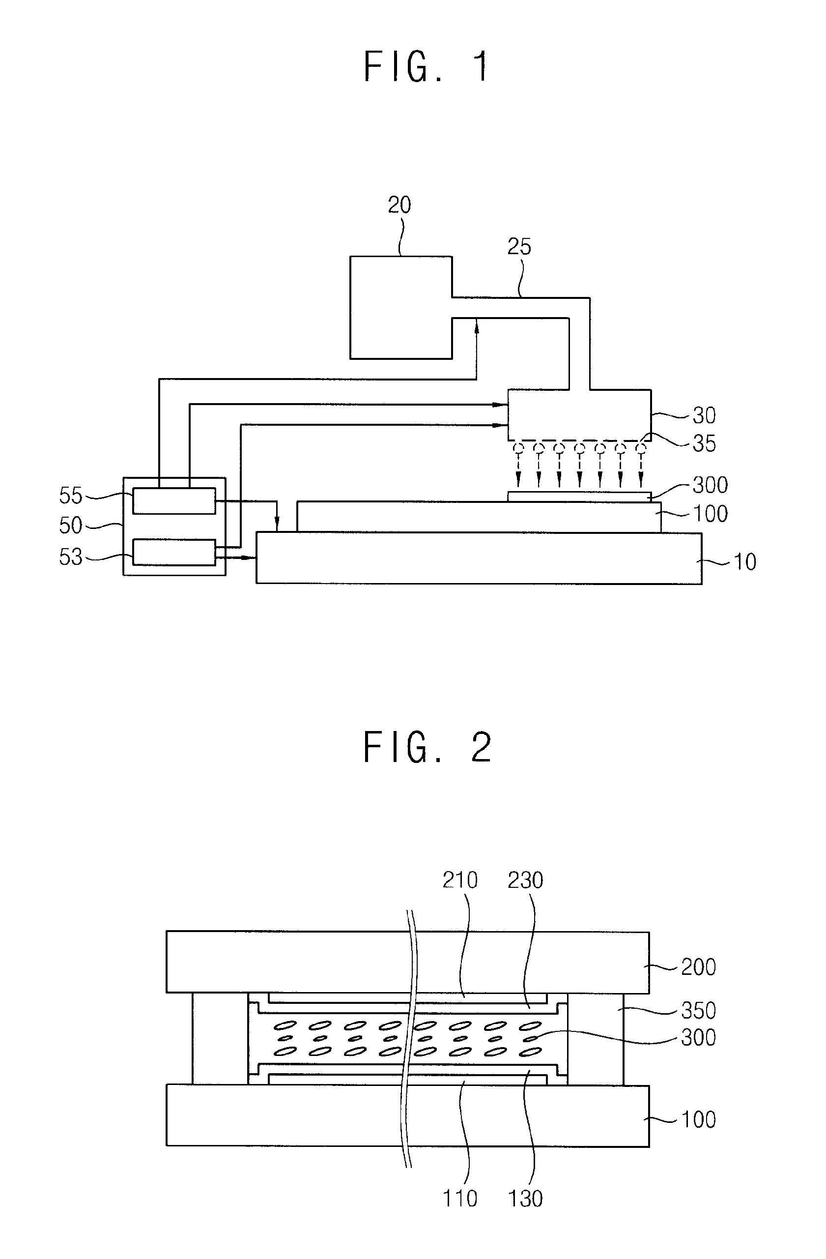
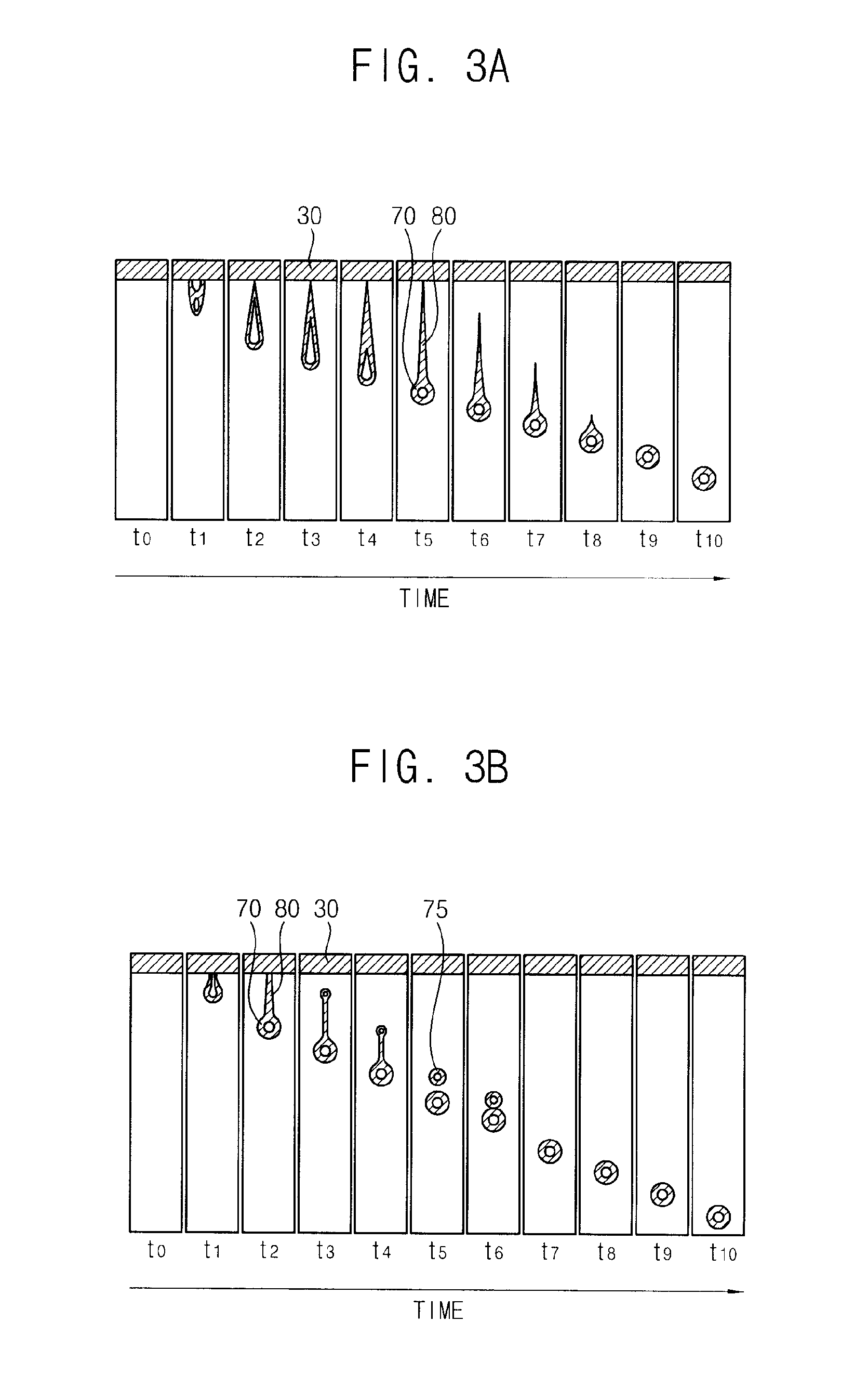
[0029]The invention is described more fully hereinafter with reference to the accompanying drawings, in which exemplary embodiments of the invention are shown. This invention may, however, be embodied in many different forms and should not be construed as limited to the exemplary embodiments set forth herein. Rather, these exemplary embodiments are provided so that this disclosure will be thorough, and will fully convey the scope of the invention to those skilled in the art. In the drawings, the size and relative sizes of layers and regions may be exaggerated for clarity. Like reference numerals in the drawings denote like elements.
[0030]It will be understood that when an element or layer is referred to as being “on,”“connected to” or “coupled to” another element or layer, it can be directly on, directly connected to, or directly coupled to the other element or layer or intervening elements or layers may be present. In contrast, when an element is referred to as being “directly on,”...
PUM
| Property | Measurement | Unit |
|---|---|---|
| temperature | aaaaa | aaaaa |
| surface tension | aaaaa | aaaaa |
| coefficient of a viscosity | aaaaa | aaaaa |
Abstract
Description
Claims
Application Information