Organic electroluminescent device
- Summary
- Abstract
- Description
- Claims
- Application Information
AI Technical Summary
Benefits of technology
Problems solved by technology
Method used
Image

Examples
example 1
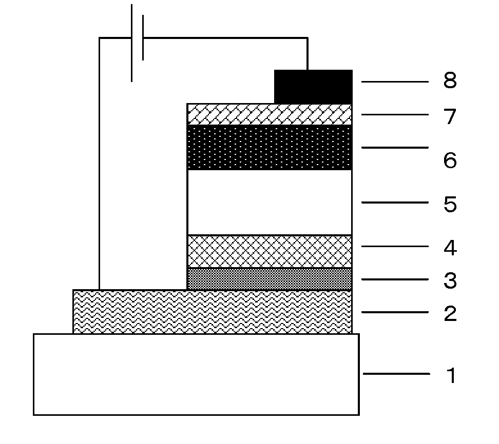
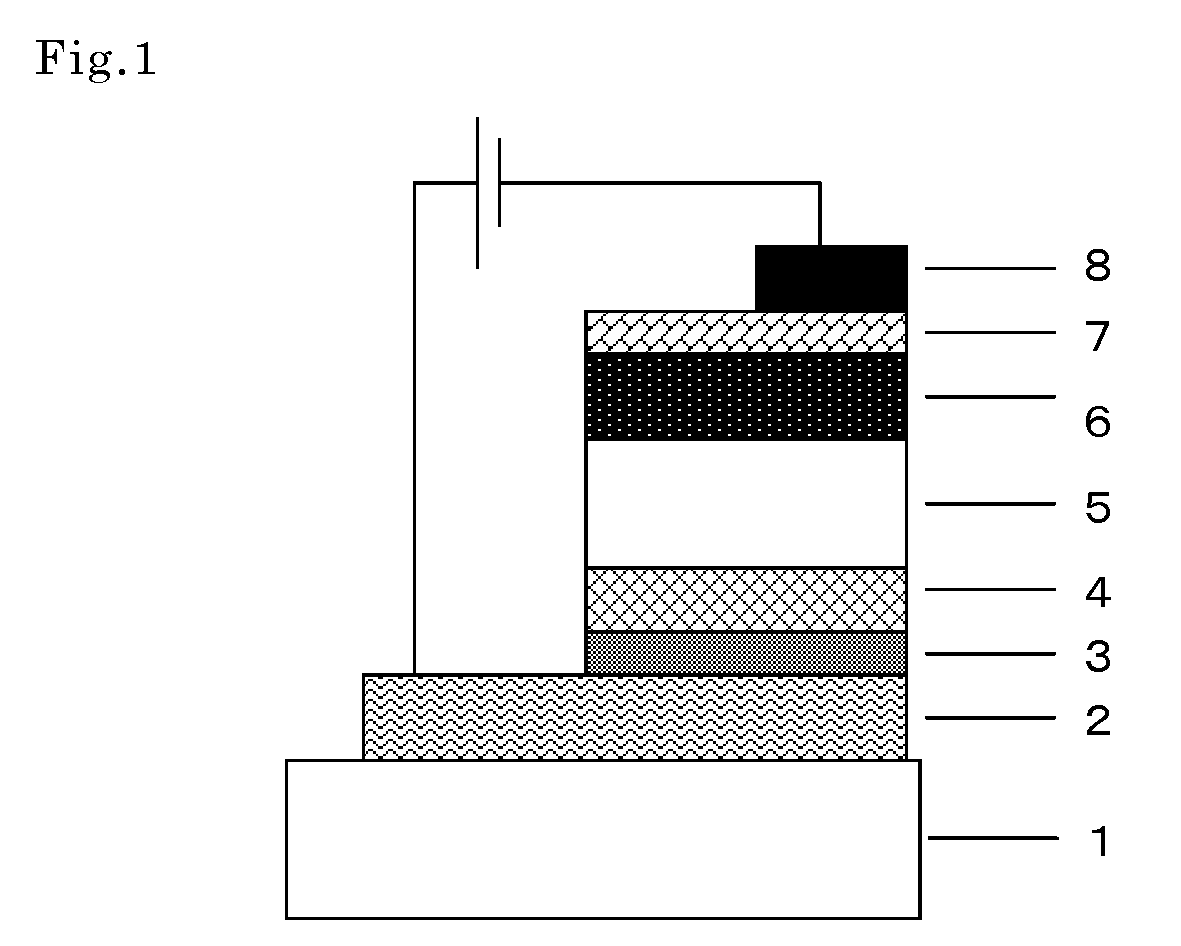
[0083]In FIG. 3, on a glass substrate, on which an anode electrode being formed of ITO and having a thickness of 150 nm had been formed, the respective thin films were laminated at a degree of vacuum of 1.0×10⁻⁵ Pa by a vacuum deposition method. First, Exemplified Compound 1 was used as a material for forming a hole-injecting layer to form a hole-injecting layer having a thickness of 10 nm on ITO. Next, 4,4′-bis(N-(1-naphthyl)-N-phenylamino)biphenyl (NPB) was used to form a hole-transporting layer having a thickness of 110 nm. Finally, aluminum (Al) was used to form a cathode electrode having a thickness of 100 nm on the hole-transporting layer. Thus, a device for evaluation of hole-injecting / transporting property was prepared.
example 2
[0084]A device for evaluation was prepared in the same manner as in Example 1 except that Exemplified Compound 14 was used as the material for a hole-injecting layer.
example 3
[0088]A device for evaluation was prepared in the same manner as in Example 1 except that the hole-injecting layer had a thickness of 20 nm and the hole-transporting layer had a thickness of 100 nm.
PUM
 Abstract
Description
Claims
Application Information
 - Generate Ideas
- Intellectual Property
- Life Sciences
- Materials
- Tech Scout
- Unparalleled Data Quality
- Higher Quality Content
- 60% Fewer Hallucinations
Browse by: Latest US Patents, China's latest patents, Technical Efficacy Thesaurus, Application Domain, Technology Topic, Popular Technical Reports.
© 2025 PatSnap. All rights reserved.Legal|Privacy policy|Modern Slavery Act Transparency Statement|Sitemap|About US| Contact US: help@patsnap.com