Touch panel apparatus and a method for detecting a contact position on the same

a touch panel and apparatus technology, applied in the field of touch panel devices, can solve the problems of high noise, delay time, and the conventional touch panel device does not output the exact contact position of the object, and achieve the effects of reducing noise, reducing noise, and reducing nois

Inactive Publication Date: 2011-05-05
ATLAB INC
View PDF10 Cites 20 Cited by
  • Summary
  • Abstract
  • Description
  • Claims
  • Application Information

AI Technical Summary

Benefits of technology

[0041]Thus, in the touch panel device and the method for detecting a contact position according to the present invention, since the plurality of touch pads are connected in series to form the touch pattern, the contact position of the entire touch panel can be sensed with only one touch sensor. Furthermore, the touch pad has a greater area than the connection line for a distinguished difference in resistance between the touch pad and the connection line, such that the contact position of the object can be easily sensed even when there is noise. In addition, the touch sensor alternately inputs the clock signal to both terminals of the touch pad in a serial connection, and calculates the contact position of the object using the delay time of the output signal, thereby minimizing the influence of noise. Furthermore, the use of the plurality of touch patterns can increase the resolution of the touch panel.

Problems solved by technology

Here, the capacitance caused by the object may also cause the delay time.
When one of the touch pad pairs with which the object is brought into contact is affected by noise, the conventional touch panel device does not output an exact contact position of the object.
Also, since each pair of rod-like touch pads 11 and 12 has resistance varying linearly with the contact position of the object, it is also highly susceptible to noise.

Method used


Image

  • Touch panel apparatus and a method for detecting a contact position on the same
  • Touch panel apparatus and a method for detecting a contact position on the same
  • Touch panel apparatus and a method for detecting a contact position on the same

Examples


Embodiment Construction

[0052]The invention is described more fully hereinafter with reference to the accompanying drawings, in which exemplary embodiments of the invention are shown.

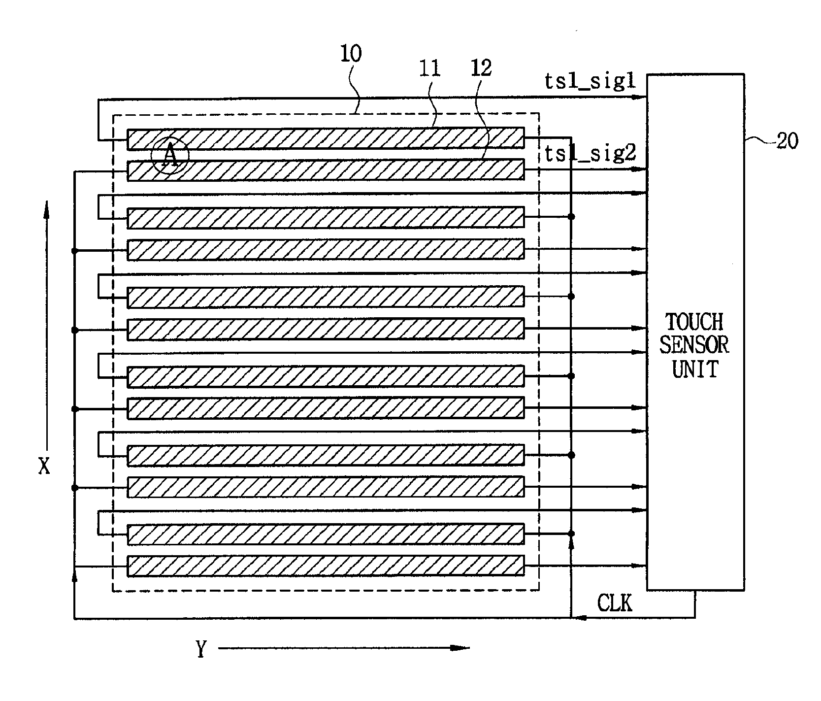
[0053]FIG. 3 illustrates a touch panel device according to a first exemplary embodiment of the present invention. The touch panel device includes an indium tin oxide (ITO) film 120 and a touch sensor 100.

[0054]In FIG. 3, a touch pattern is formed on one entire surface of the ITO film 120. The touch pattern includes a plurality of touch pads P1_1 to P1_(n) and a plurality of connection lines CL1_1 to CL1_(n−1), each having predetermined resistance. Each of the touch pads P1_1 to P1_(n) is connected in series with adjacent touch pads by corresponding ones of the connection lines CL1_1 to CL1_(n−1). The plurality of connection lines CL1_1 to CL1_(n−1) may be formed of conductors. However, it is assumed herein that the plurality of connection lines CL1_1 to CL1_(n−1) are formed by ITO patterning, like the touch pads P1_1 to P1_(n)...


PUM


Abstract

A touch panel device and a method for detecting a contact position are provided. The touch panel device includes a touch panel including a first touch pattern, the first touch pattern having a plurality of first touch pads connected in series; and a touch sensor for applying a clock signal to one terminal of the first touch pattern, receiving a first delayed clock signal from the other terminal of the first touch pattern, and generating contact position data corresponding to a contact position of an object using a difference in delay time between the clock signal and the first delayed clock signal. Thus, since the plurality of touch pads are connected in series, the contact position of the entire touch panel can be sensed with only one touch sensor, and the touch pad has a greater area than the connection line for a distinguished difference in resistance between the touch pad and the connection line, such that the contact position can be accurately detected.

Description

TECHNICAL FIELD[0001]The present invention relates to a touch panel device, and more particularly, to a touch panel device with a reduced number of touch sensors, and a method for detecting a contact position on the touch panel.BACKGROUND ART[0002]An indium tin oxide (ITO) film is widely used as a transparent electrode (film) for display devices, such as liquid crystal displays. The ITO has been applied as an electrode material to devices from several fields, such as liquid crystal display (LCD) devices, organic light emitting diodes, solar cells, plasma displays, E-Papers, and the like because of its high transparency and low sheet resistance as a thin transparent conductive oxide film, and easy patterning. It has also been applied to reduce electro-magnetic interference for a cathode ray tube (CRT) monitor, and ITO ink.[0003]A touch panel device using ITO is described in Korean Patent Publication No. 10-2007-0112750.[0004]FIG. 1 illustrates a configuration of a conventional touch ...

Claims


Application Information

Patent Timeline
Patent Type & Authority Applications(United States)
IPC IPC(8): G06F3/041
CPCG06F3/041G06F3/044G06F3/045G06F3/0443G06F3/04166G06F3/0354G06F3/04182
Inventor KIM, BOM-YUNJUNG, DUCK-YOUNGLEE, SANG-JINJOUNG, CHUL-YONGCHUNG, JIN-WOOSHIN, YOUNG-HOLEE, BANG-WON
Owner ATLAB INC
Why Eureka
Try Eureka