Active matrix electroluminescent display with segmented electrode

a technology of active matrix and segmented electrodes, applied in the field of active matrix electroluminescent (el) display, can solve the problems of inability to independently control the current to each element of either electrode, significant power loss, and limited practicality of passive matrix el displays, so as to improve the effective resolution of active-matrix electroluminescent display and reduce the power consumption of the display

Inactive Publication Date: 2011-05-05
GLOBAL OLED TECH
View PDF18 Cites 16 Cited by
  • Summary
  • Abstract
  • Description
  • Claims
  • Application Information

AI Technical Summary

Benefits of technology

[0014]The arrangement of the present invention provides the advantages of improving the effective resolution of the active-matrix electroluminescent display, without increasing the number of active matrix drive circuits within the display. Additionally, this arrangement can be provided with optical lenses to reduce the power consumption of the display or provide sets of image data.

Problems solved by technology

However, to avoid cross talk and to provide distinct currents to each light-emitting element, current can only be provided to one electrode strip, typically the cathode, within one direction, typically the row direction, at any instant in time.
Because each light-emitting element preferably produces light at least 60 times per second to avoid flicker, and because each light-emitting element has a very significant capacitance, significant power losses occur if the passive-matrix display is large or high in resolution.
Therefore, passive matrix EL displays are often only practical when forming small or low resolution displays.
However, it is not possible to independently control the current to every element of either electrode through active circuits and therefore Komatsu et al clearly provides a passive matrix display.
Displays employing high resolution arrays of these active matrix drive circuits are complex to make and the active matrix circuits typically require significant space on the display substrate.
Further, defects are likely when forming the hundreds of thousands or millions of transistors that are required to form such a display and the likelihood of a defect increases with increasing numbers of transistors.
Therefore, increasing the resolution of the display by increasing the number of active-matrix circuits typically results in lower yields of marketable displays from manufacturing and, therefore, increases the manufacturing cost of the display.
Unfortunately, the resolution of each image is reduced by a factor equal to the inverse of the number of different directions and therefore, these methods reduce the effective resolution of the display device.
As with barrier screens, these type of screens reduce the effective resolution of the display when presenting multi-view stereo images.
Therefore, this approach can be expensive to implement, and can require a lower-resolution display to achieve acceptable update rates.
Unfortunately, display technologies that are commercially available today have limited update rates, which would limit the number of views provided by such a method.
Unfortunately, such a display requires a large number of individually-addressable light-emitting elements within each pixel.
Moreover, with the technology available today, it is not possible to create a high-resolution display having numerous, individually-addressable light-emitting elements within each pixel.

Method used


Image

  • Active matrix electroluminescent display with segmented electrode
  • Active matrix electroluminescent display with segmented electrode
  • Active matrix electroluminescent display with segmented electrode

Examples


Embodiment Construction

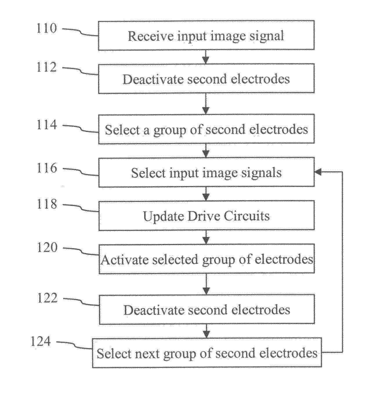
[0025]The present invention provides an electroluminescent (EL) display having a larger number of individually-addressable light-emitting elements than the number of active-matrix circuits for providing current to each individual light-emitting element.

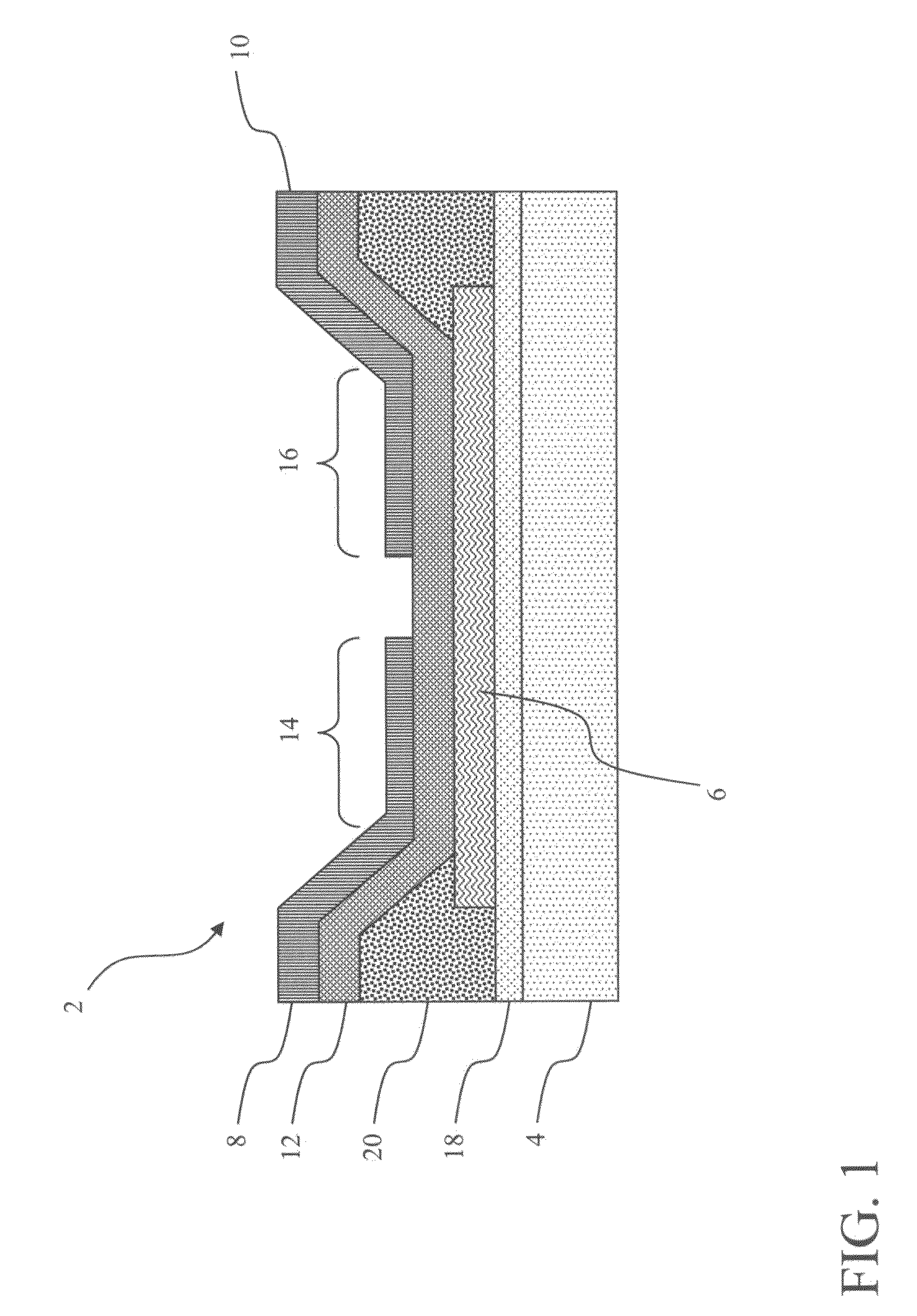
[0026]The present invention provides an active-matrix electroluminescent display. This active-matrix electroluminescent display includes a display panel 2, a portion of which is shown in FIG. 1. This display panel 2 includes a display substrate 4. At least a first electrode 6 is disposed over an area of the display substrate 4. Two or more individually-addressable, second electrodes 8, 10 are further disposed over the display substrate 4 and the first electrode 6. An electroluminescent light-emitting layer 12 is formed between and in electrical contact with the first 6 and each of the second 8, 10 electrodes, so that first and second active areas 14, 16 are defined where the first electrode 6 and each respective second electrode 8, 10...


PUM


Abstract

An active-matrix electroluminescent display including a display substrate; a first electrode disposed over the display substrate; two second electrodes disposed over the first electrode; an electroluminescent light-emitting layer formed between and in electrical contact with the first and second electrodes, so that first and second active areas are defined where the first electrode and each respective second electrode overlap, the light-emitting layer emitting light from each active area in response to current between the first and each respective second electrode; a drive circuit including a drive transistor electrically connected to the first electrode for controlling the flow of current through the electroluminescent light-emitting layer; two power supply circuits connected to respective second electrodes for selectively providing respective voltages to the respective second electrodes; and a controller for sequentially or simultaneously causing the power supply circuits to provide the voltages to the respective second electrodes.

Description

CROSS REFERENCE TO RELATED APPLICATIONS[0001]Reference is made to commonly-assigned U.S. patent application Ser. No. 12 / 191,478 filed Aug. 14, 2008 entitled “OLED Device With Embedded Chip Driving” to Dustin L. Winters et al.; U.S. patent application Ser. No. 11 / 959,755 (U.S. Patent Application Publication No. 2009 / 0160826) filed Dec. 19, 2007 entitled “Drive Circuit And Electro-Luminescent Display System” to Michael E. Miller et al., and U.S. patent application Ser. No. 11 / 936,251 (U.S. Patent Application Publication No. 2009 / 0115705) filed Nov. 7, 2007 entitled “Electro-Luminescent Display Device” to Michael E. Miller et al., the disclosures of which are incorporated herein.FIELD OF THE INVENTION[0002]The present invention relates to an active matrix electroluminescent (EL) display having a segmented top electrode wherein the electrode segments are driven to provide an increased resolution. Several applications of this EL display are discussed, including a reduced power EL display...

Claims


Application Information

Patent Timeline
Patent Type & Authority Applications(United States)
IPC IPC(8): G09G5/00H05B44/00
CPCG09G3/3233G09G2300/0426G09G2300/0842H01L51/5275H01L27/3246H01L51/5221G09G2330/021H10K59/122H10K50/82H10K50/858G09F9/301H10K50/13H10K50/11H10K2102/302
Inventor HAMER, JOHN W.MILLER, MICHAEL E.
Owner GLOBAL OLED TECH
Why Eureka
Try Eureka