Load driving device
a technology of load driving device and load current, which is applied in the direction of semiconductor devices, transistors, pulse techniques, etc., can solve the problems of increasing the consumption current of the load driving device of the prior art, unable to operate normally for each transistor, and generating consumption current, so as to prevent the breakdown of the load driving device and suppress heat generation. , the effect of suppressing the increase in consumption curren
- Summary
- Abstract
- Description
- Claims
- Application Information
AI Technical Summary
Benefits of technology
Problems solved by technology
Method used
Image

Examples
first exemplary embodiment
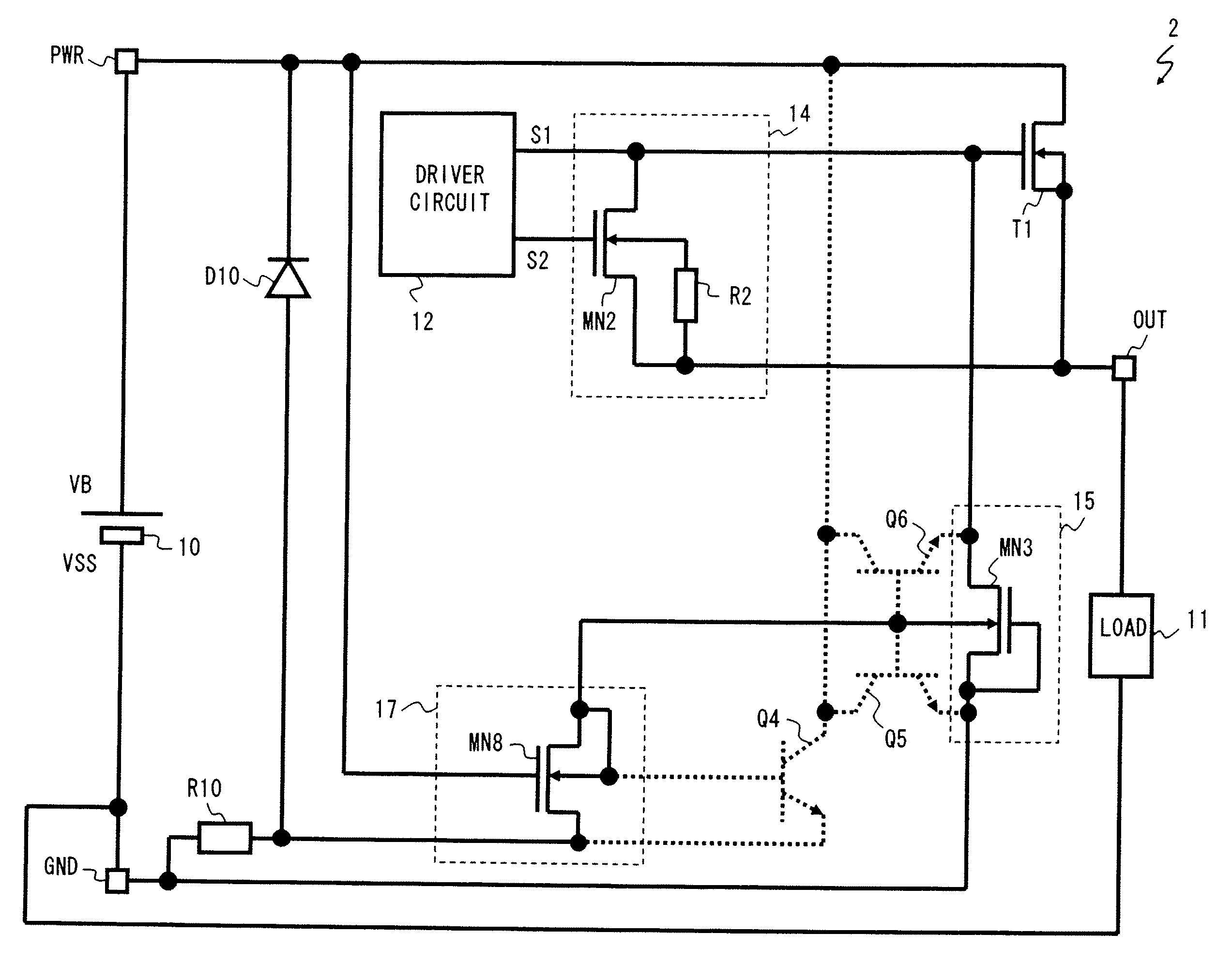
[0043]FIG. 1 shows a circuit diagram of a load driving device 2 according to a first exemplary embodiment of the present invention. As shown in FIG. 1, the load driving device 2 includes a power supply 10, a load 11, a driver circuit 12, a gate discharge circuit 14, a reverse connection protection circuit 15, a back gate control circuit 17, an output transistor T1, a clamp diode (protection diode) D10, a current restriction resistor R10, a power supply terminal PWR, a ground terminal GND, and an output terminal OUT. In the first exemplary embodiment, a power supply line that couples the power supply 10 and the output transistor T1 through the power supply terminal PWR is referred to as a first power supply line, and a power supply line that couples the power supply 10 through the ground terminal GND is referred to as a second power supply line.
[0044]The power supply 10 is coupled between the power supply terminal PWR and the ground terminal GND. At a time of normal connection, the p...
second exemplary embodiment
[0091]A load driving device 3 according to a second exemplary embodiment of the present invention will be described with reference to the drawings. The load driving device 3 includes a back gate control circuit 17b which is a modified example of the back gate control circuit 17 according to the first exemplary embodiment. The load driving device 3 also includes a reverse connection protection circuit 15b which is a modified example of the reverse connection protection circuit 15 according to the first exemplary embodiment. The components of the load driving device 3 that are similar to those of the load driving device 2 are denoted by the same reference symbols, and the description thereof is omitted.
[0092]In comparison with the back gate control unit 17 of the load driving device 2, the back gate control circuit 17b of the load driving device 3 causes the back gate of the protection transistor MN3 to be short-circuited to the potential of the output terminal OUT with a low impedanc...
third exemplary embodiment
[0115]FIG. 9 shows a circuit diagram of a load driving device 4 according to a third exemplary embodiment of the present invention. FIG. 10 shows a sectional view of devices constituting the load driving device 4 according to the third exemplary embodiment. FIG. 11 shows a circuit diagram of the load driving device 4 at the time of reverse connection of a power supply. FIG. 12 shows a sectional view of the devices constituting the load driving device 4 at the time of reverse connection of the power supply.
[0116]The load driving device 4 is a modified example of the load driving device 2, in which the first N-type MOS transistor MN8 is replaced by a diffusion resistor (a first resistor) R4. The functions of the load driving device 4 can be implemented by a smaller number of constituent elements than the load driving device 2.
[0117]A back gate control circuit 17c of the load driving device 4 includes the resistor R4. More specifically, the resistor R4 has one terminal coupled to the a...
PUM
 Abstract
Description
Claims
Application Information
 - R&D
- Intellectual Property
- Life Sciences
- Materials
- Tech Scout
- Unparalleled Data Quality
- Higher Quality Content
- 60% Fewer Hallucinations
Browse by: Latest US Patents, China's latest patents, Technical Efficacy Thesaurus, Application Domain, Technology Topic, Popular Technical Reports.
© 2025 PatSnap. All rights reserved.Legal|Privacy policy|Modern Slavery Act Transparency Statement|Sitemap|About US| Contact US: help@patsnap.com