

Observation device and observation method
a technology of observation device and observation method, which is applied in the direction of semiconductor/solid-state device testing/measurement, instruments, television systems, etc., can solve the problem of affecting the yield of circuit elements created from wafers, and achieve the effect of high precision
- Summary
- Abstract
- Description
- Claims
- Application Information
AI Technical Summary
Benefits of technology
Problems solved by technology
Method used
Image

Examples
Embodiment Construction
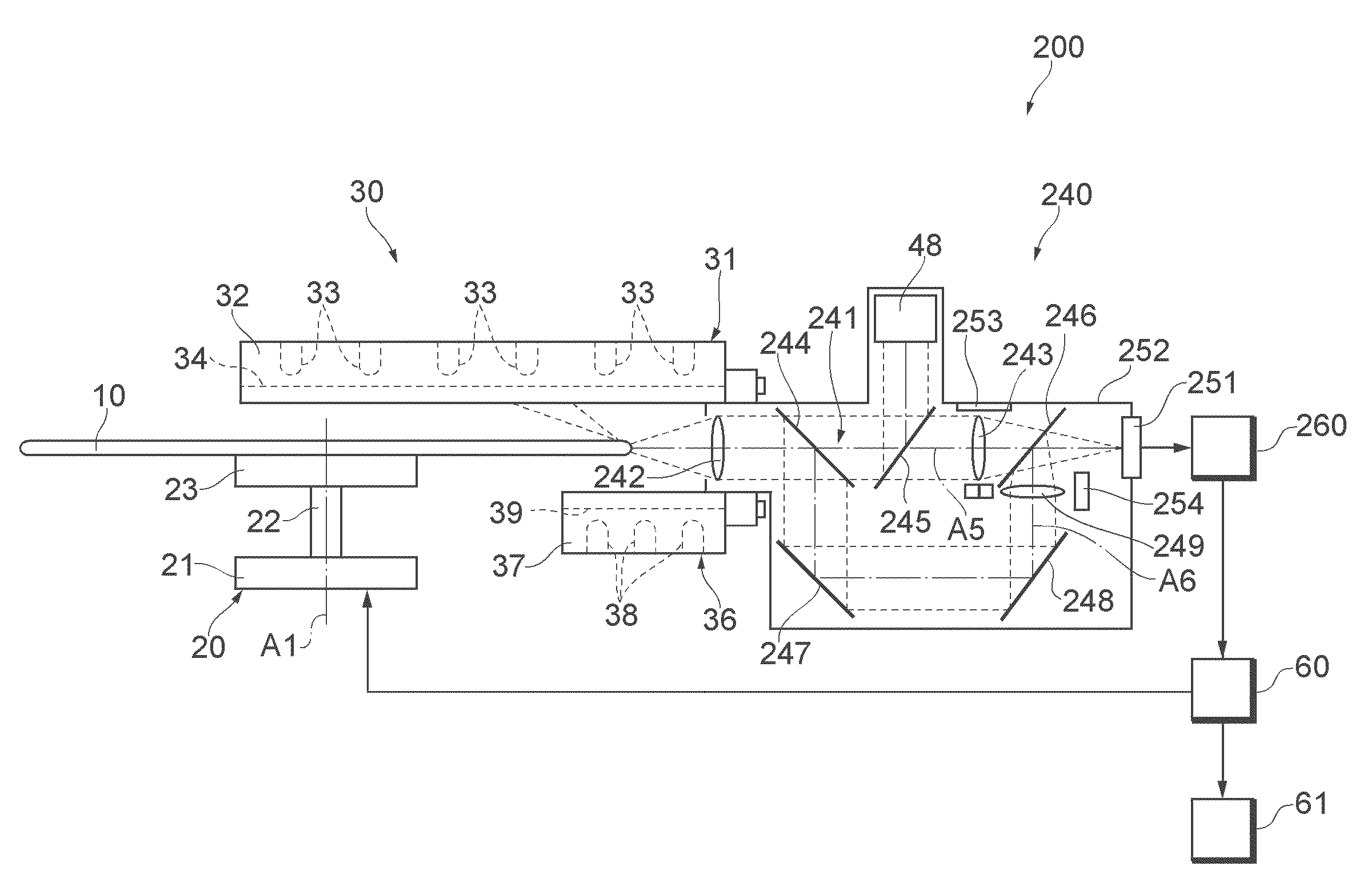
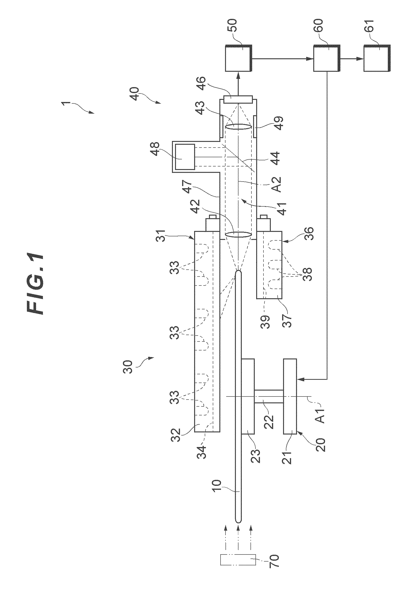
[0033]Preferred embodiments of the present invention are described below. An example of the observation device according to the present invention is shown in FIG. 1, and the observation device 1 is used for visual observation by an observer to detect the presence of abnormalities in an end or near the end of a semiconductor wafer 10 (hereinafter referred to as “wafer 10”).
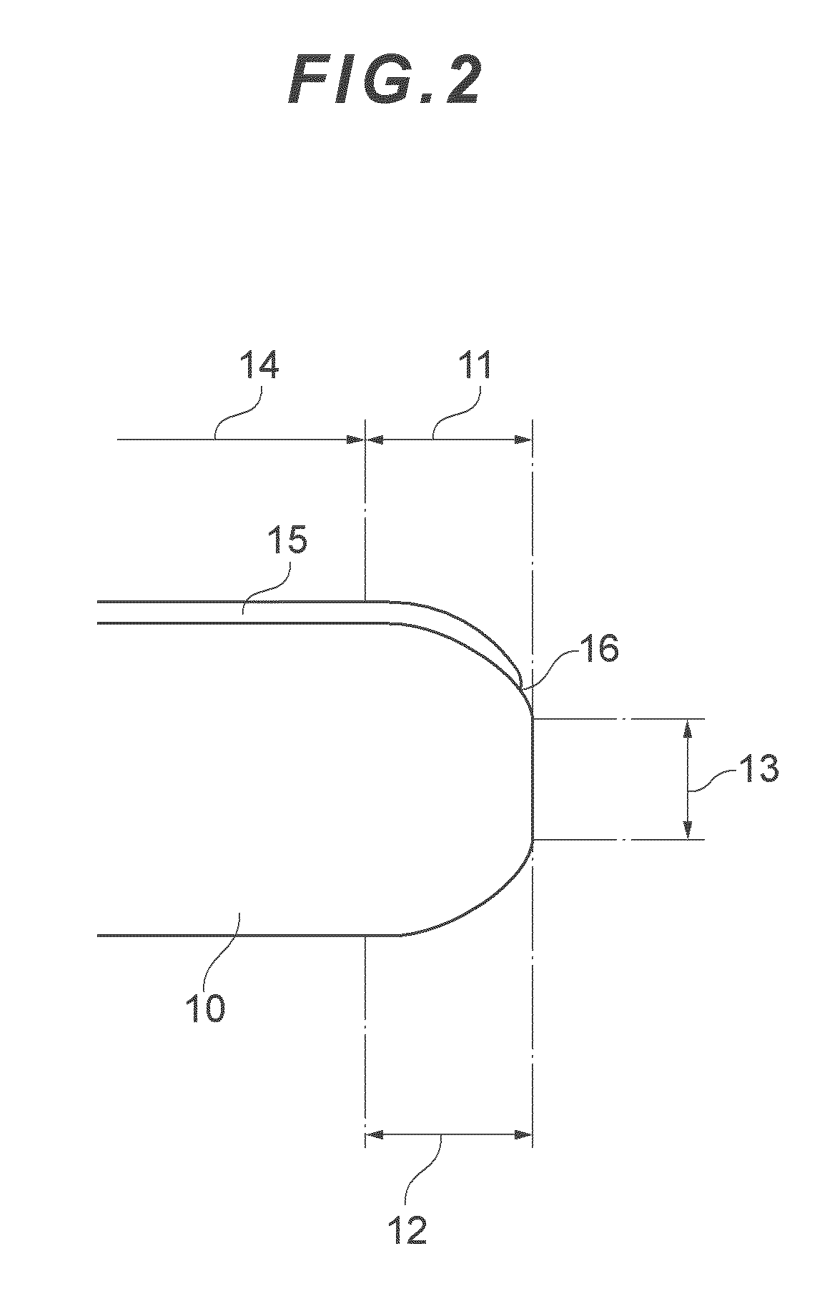
[0034]The wafer 10, which is a substrate, is formed in a thin circular shape, and a thin protective film 15 is formed on the surface thereof, as shown in FIG. 2. An upper bevel portion 11 that slopes facing the external peripheral end side of the wafer 10 is formed in the shape of a ring inside the external peripheral end in the surface (upper surface) of the wafer 10, and a flat portion 14 that is substantially flat is formed inside the upper bevel portion 11. Also, a lower bevel portion 12 is formed in obverse / reverse symmetry with the upper bevel portion 11 about the wafer 10 inside the external peripheral end o...
PUM
 Abstract
Description
Claims
Application Information