Method for predicting and warning of wafer acceptance test value

a technology of acceptance test and wafer, applied in the direction of electric/magnetic computing, semiconductor/solid-state device testing/measurement, instruments, etc., can solve the problems of process faults, inability to test all wafers, and inability to control the quality of all wafers. certain and fully

Inactive Publication Date: 2011-05-12
INOTERA MEMORIES INC
View PDF3 Cites 9 Cited by
  • Summary
  • Abstract
  • Description
  • Claims
  • Application Information

AI Technical Summary

Benefits of technology

[0008]It is therefore an object of the invention to provide a method for predicting and warning of WAT (Wafer Acceptance Test) value, which can predict accurately the WAT (Wafer Acceptance Test) value and does not need

Problems solved by technology

The semiconductor wafer manufacturing yield closely affects the product cost and industry competition, so that the semiconductor industries unceasingly endeavor and research to improve and raise the yield as their goal.
The fabrication of ICs on the wafer requires that the wafer 100 undergo a large number of relatively complex process steps, with potential process faults occurring at each process step.
However, the WAT (Wafer Accept

Method used


Image

  • Method for predicting and warning of wafer acceptance test value
  • Method for predicting and warning of wafer acceptance test value
  • Method for predicting and warning of wafer acceptance test value

Examples


Embodiment Construction

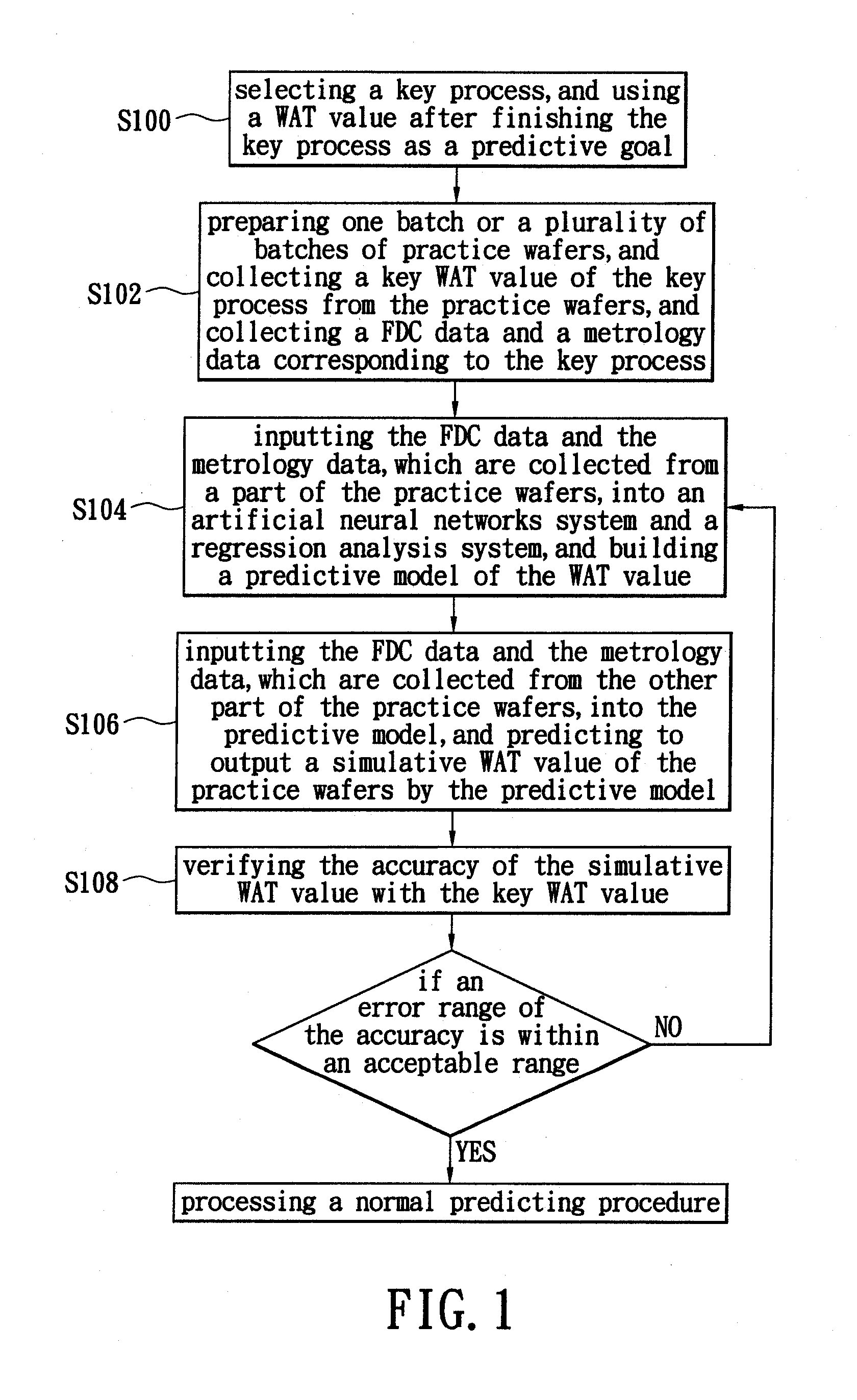
[0020]Reference is made to FIGS. 1 and 2. The present invention provides a method for predicting and warning of WAT (Wafer Acceptance Test) value, which includes the steps as follows. First, as shown in FIG. 1, a training procedure needs to be performed ahead, so as to build a predicting model. Then, as shown in FIG. 2, a predicting procedure is performed accordingly.

[0021]Reference is made to FIG. 1. The training procedure is performed in advance, which includes steps as follows. First, in step S100, a key process, which crucially affects quality among the manufacturing processes, is selected. For example, a typical wafer that starts out being a raw wafer may undergo the following processes: deposition, masking, etching, doping, metallization, and passivation. The key process, for example, would be the gate oxidation etching process, etc. A WAT (Wafer Acceptance Test) value after the key process finished is used as a predicted goal. Next, in step S102, one hundred batches of practi...


PUM


Abstract

A method for predicting and warning of WAT value includes the steps as follows. A key process is selected and a WAT value after finishing the key process is used as a predictive goal. A predicting model is built. One batch or plural batches of predictive wafers are prepared, and a Fault Detection and Classification data (FDC data) and a metrology data from the predictive wafers of the key process are collected. The FDC data and the metrology data collected from the predictive wafers are inputted into the predicting model for processing a normal predicting procedure, and a predictive WAT value by the predicting model is outputted. The present invention can accurately predict the WAT value, effectively monitor some specific defective wafers and continuously perform the improvement for the specific defective wafer.

Description

BACKGROUND OF THE INVENTION[0001]1. Field of the Invention[0002]The present invention relates to a method for predicting and warning of WAT (Wafer Acceptance Test) value, and more particularly to a method which can accurately predict the WAT (Wafer Acceptance Test) value during manufacturing process without any practical test after a predicting model of WAT (Wafer Acceptance Test) value is built, and warning the relative responsible person of abnormal WAT (Wafer Acceptance Test) value.[0003]2. Description of Related Art[0004]The semiconductor wafer manufacturing yield closely affects the product cost and industry competition, so that the semiconductor industries unceasingly endeavor and research to improve and raise the yield as their goal. The fabrication of ICs on the wafer requires that the wafer 100 undergo a large number of relatively complex process steps, with potential process faults occurring at each process step. In semiconductor fabrication processes, the WAT (Wafer Accep...

Claims


Application Information

Patent Timeline
IPC IPC(8): G06N3/10G06F15/18
CPCH01L22/20
Inventor LEE, YI-FENGKAO, SHIH CHANGTIAN, YUN-ZONGCHEN, WEI JUN
Owner INOTERA MEMORIES INC
Why Eureka
Try Eureka