
Nanofabrication process and nanodevice

a nanofabrication and nanotechnology, applied in the field of nanofabrication process and nanofabrication device, can solve the problems of limiting the design and functionality of the device, limiting the dimensional limitations on serial patterning and alignment limit the geometry, number and size of channel depths that can be formed,

Active Publication Date: 2011-05-26
CORNELL UNIV CORNELL CENT FOR TECH ENTERPRISE & COMMLIZATION CCTEC
View PDF9 Cites 13 Cited by
  • Summary
  • Abstract
  • Description
  • Claims
  • Application Information

AI Technical Summary

Problems solved by technology

Moreover, features from different iterations must overlap to form a continuous channel, which can result in multiple etches in the overlapping region that limit device design and functionality.
The inherent dimensional limitations on serial patterning and alignment limit the geometry, number and size of the channel depths that can be formed and prevent the fabrication of some complex three dimensional surface features.
Indeed, since the utility of a nanodevice is in general proportional to its complexity and dimensionality, current devices provide relatively limited ability to manipulate biomolecules or other analytes of interest.

Method used


Image

  • Nanofabrication process and nanodevice
  • Nanofabrication process and nanodevice
  • Nanofabrication process and nanodevice

Examples


Embodiment Construction

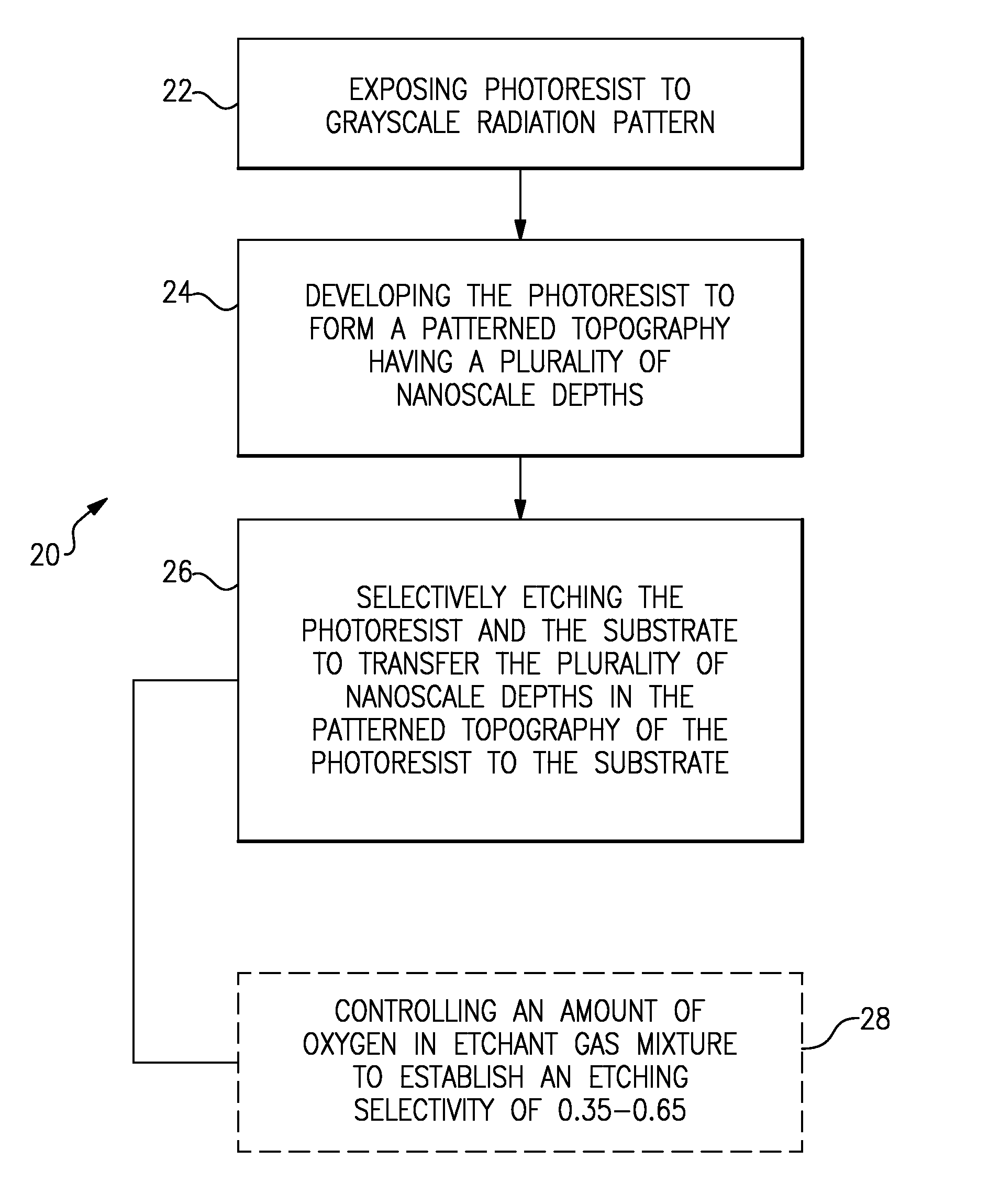
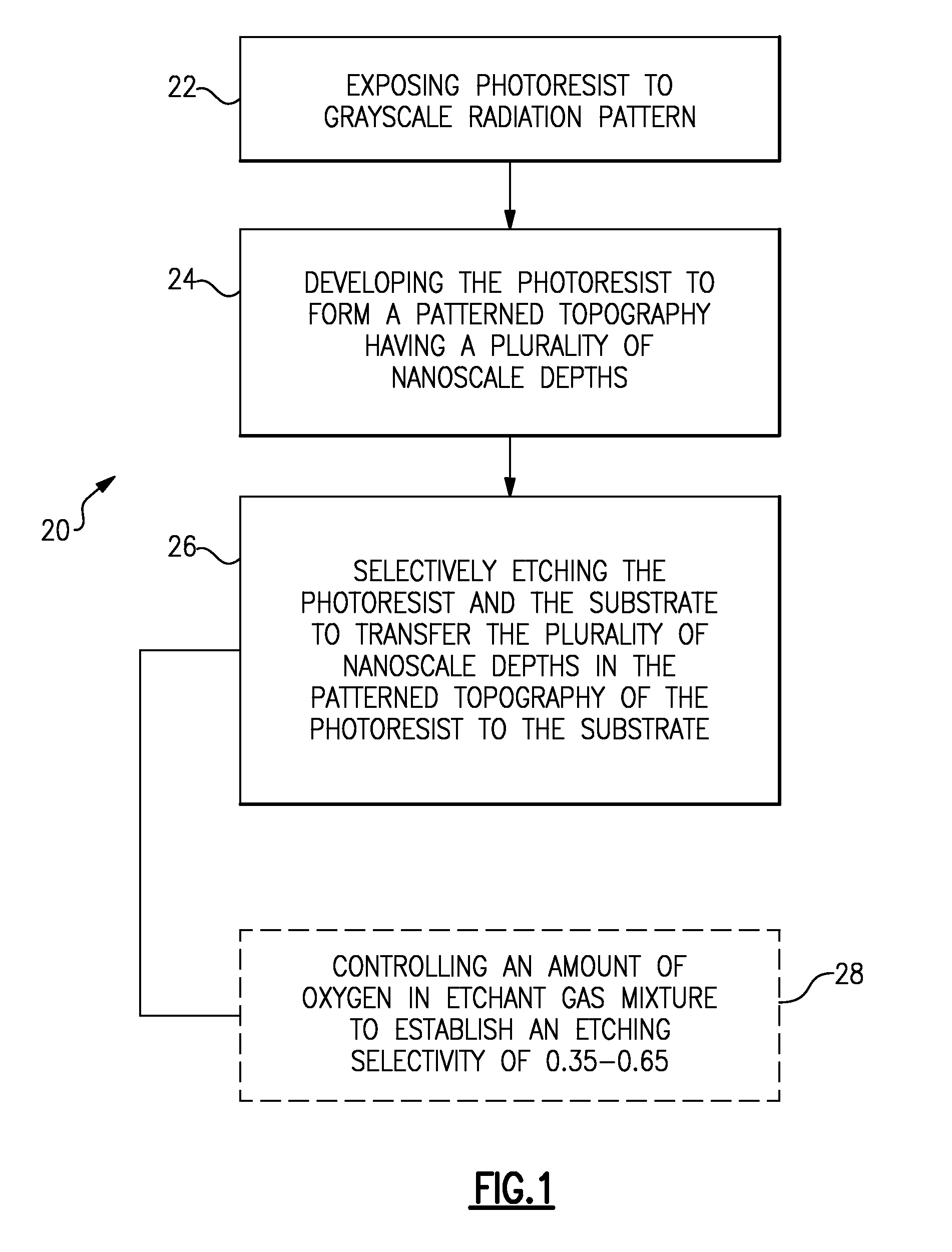
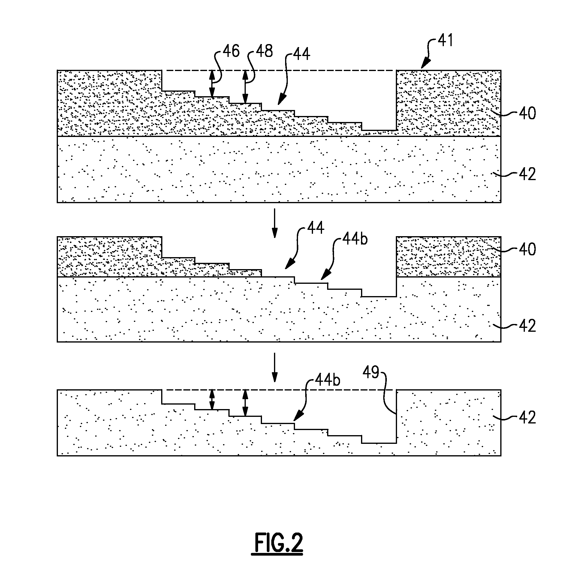
[0012]FIG. 1 illustrates an example of nanofabrication process 20 that may be used with a photoresist that is disposed on a substrate to form a nanodevice. As will be appreciated from the following description, the nanofabrication process 20 may be adapted to form a variety of different types of nanodevices that are unavailable using conventional techniques. In a few examples, the nanofabrication process 20 may be used to form a nanofluidic device, integrated circuit, nanomolding tool, resonator, or other device that would benefit from the ability to form complex three dimensional surface topographies defined by a plurality of nanometer scale or nanoscale critical dimensions. As an example, the terms “nanometer scale” or “nanoscale” may refer to a critical dimension or characteristic dimension of up to about one-hundred nanometers. In comparison, larger dimensions of up to one micrometer may be referred to as “submicrometer” and dimensions exceeding one micrometer and up to about on...


PUM

PropertyMeasurementUnit
step heightsaaaaaaaaaa
surface roughnessaaaaaaaaaa
thicknessaaaaaaaaaa

Abstract

A nanofabrication process for use with a photoresist that is disposed on a substrate includes the steps of exposing the photoresist to a grayscale radiation pattern, developing the photoresist to remove a irradiated portions and form a patterned topography having a plurality of nanoscale critical dimensions, and selectively etching the photoresist and the substrate to transfer a corresponding topography having a plurality of nanoscale critical dimensions into the substrate.

Description

BACKGROUND OF THE INVENTION[0001]This disclosure relates to processes for patterning and etching a substrate to form a complex three dimensional surface topography defined by a plurality of nanometer scale critical dimensions and devices manufactured using such processes.[0002]Lithography (e.g., photolithography) is known and used for fabricating nanofluidic devices, integrated circuits, and the like. As an example, a typical nanofluidic device may include a fluidic channel with a nanometer scale depth for the manipulation and analysis of biomolecules, such as nucleic acids and proteins.[0003]Currently, photolithography is one method that is used to fabricate such nanofluidic channels. For instance, a photoresist layer may be deposited onto a substrate and then exposed to a light pattern created using a photomask. The portions of the photoresist that are exposed to the light are either rendered resistant to a developer (i.e., when a negative photoresist is used) or soluble in the de...

Claims


Application Information

Patent Timeline
Patent Type & Authority Applications(United States)
IPC IPC(8): B32B3/30B44C1/22
CPCB82Y30/00Y10T428/24479B81B1/006G03F7/40
Inventor STAVIS, SAMUEL MARTINSTRYCHALSKI, ELIZABETH ARLENEGAITAN, MICHAEL
Owner CORNELL UNIV CORNELL CENT FOR TECH ENTERPRISE & COMMLIZATION CCTEC
Learn More