
Photovoltaic solar module comprising bifacial solar cells
a solar cell and photovoltaic technology, applied in the direction of pv power plants, manufacturing tools, soldering apparatus, etc., can solve the problem that the amount of silicon used directly affects manufacturing costs, and achieve the effect of less costly, less cost, and compromising the structural integrity of solar cells
- Summary
- Abstract
- Description
- Claims
- Application Information
AI Technical Summary
Benefits of technology
Problems solved by technology
Method used
Image

Examples
Embodiment Construction
[0031]Reference will now be made in detail to exemplary embodiments of the present invention, with further reference to the accompanying drawings. It will be apparent to those skilled in the art that various modifications and variations are possible without departing from the spirit or scope of the invention.
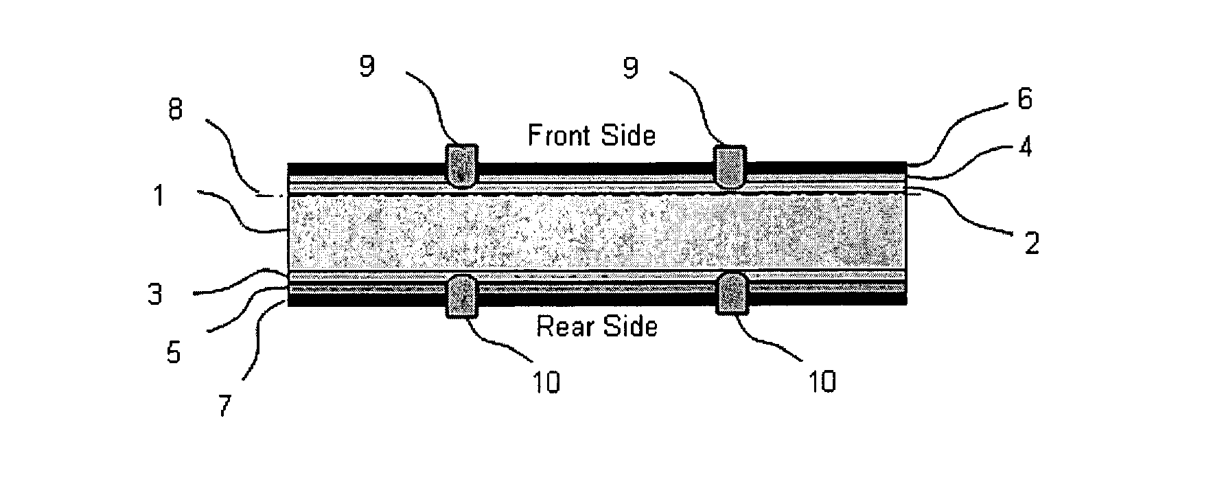
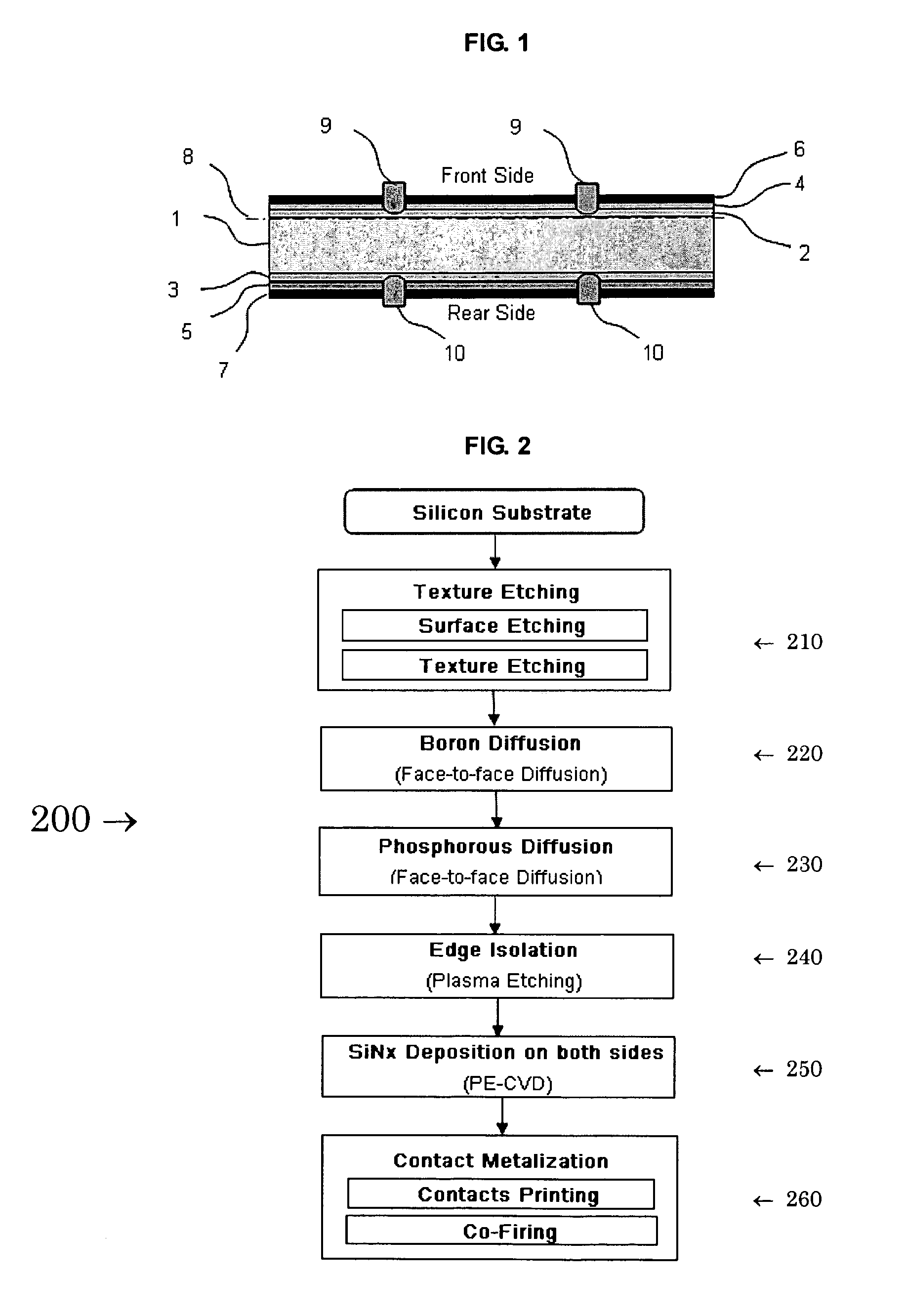
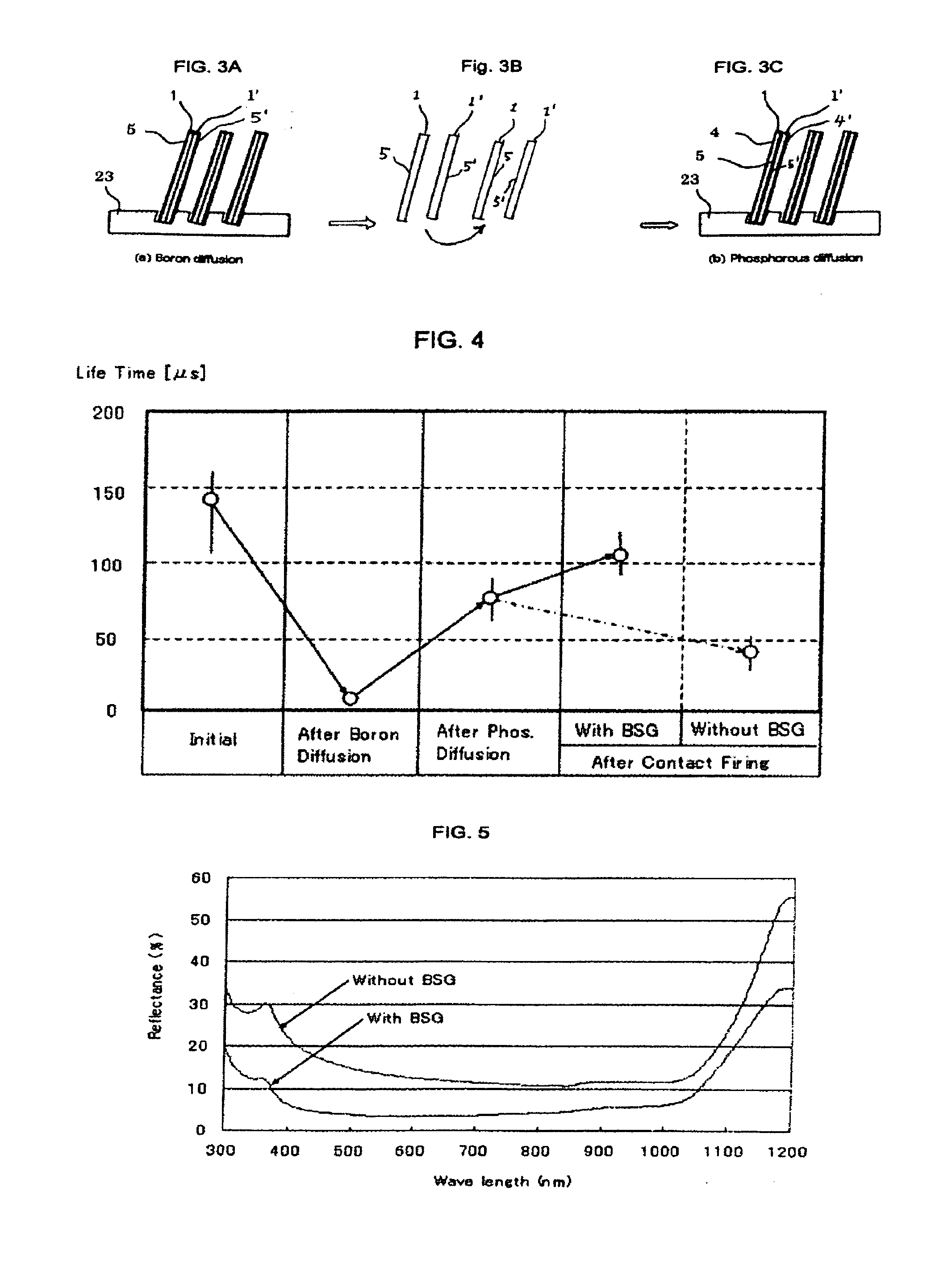
[0032]FIG. 1 illustrates a cross sectional view of an exemplary bifacial solar cell. The bifacial solar cell comprises a silicon substrate 1. The silicon substrate 1 can be mono-crystalline silicon, multi-crystalline silicon, or another similar semiconductor material, and it can be either p- or n-type. The silicon substrate 1 here is a p-type substrate, as an example. The silicon substrate 1 is coated with an n+ layer 2 on the front side and a p+ layer 3 on the rear side. A phosphorous silicon glass (PSG) layer 4 is deposited on the n+ layer 2. A boron silicon glass (BSG) layer 5 is deposited on the p+ layer 3. The junction 8, which forms a diode in the bifacial solar cell, is a...
PUM
| Property | Measurement | Unit |
|---|---|---|
| Temperature | aaaaa | aaaaa |
| Temperature | aaaaa | aaaaa |
| Temperature | aaaaa | aaaaa |
Abstract
Description
Claims
Application Information