SRAM Structure with FinFETs Having Multiple Fins

Active Publication Date: 2011-06-09
TAIWAN SEMICON MFG CO LTD
View PDF21 Cites 67 Cited by
  • Summary
  • Abstract
  • Description
  • Claims
  • Application Information

AI Technical Summary

Benefits of technology

In accordance with one aspect, a static random access memory (SRAM) cell includes a straight fin and a bended fin physically disconnected from the straight fin. The bended fin has a first portion and a second portion parallel to the straight fin. The distance between the first portion of the bended fin and the straight fin is smaller than the distance between the second portion of the bended fin and the straight fin. The SRAM cell include

Problems solved by technology

The SRAMs with single-fin FinFETs, however, often suffer from low cell ratio problems such as low beta ratios.
In the formation of high-density SRAM arrays, ho

Method used


Image

  • SRAM Structure with FinFETs Having Multiple Fins
  • SRAM Structure with FinFETs Having Multiple Fins
  • SRAM Structure with FinFETs Having Multiple Fins

Examples


Embodiment Construction

The making and using of the embodiments of the disclosure are discussed in detail below. It should be appreciated, however, that the embodiments provide many applicable inventive concepts that can be embodied in a wide variety of specific contexts. The specific embodiments discussed are merely illustrative of specific ways to make and use the embodiments, and do not limit the scope of the disclosure.

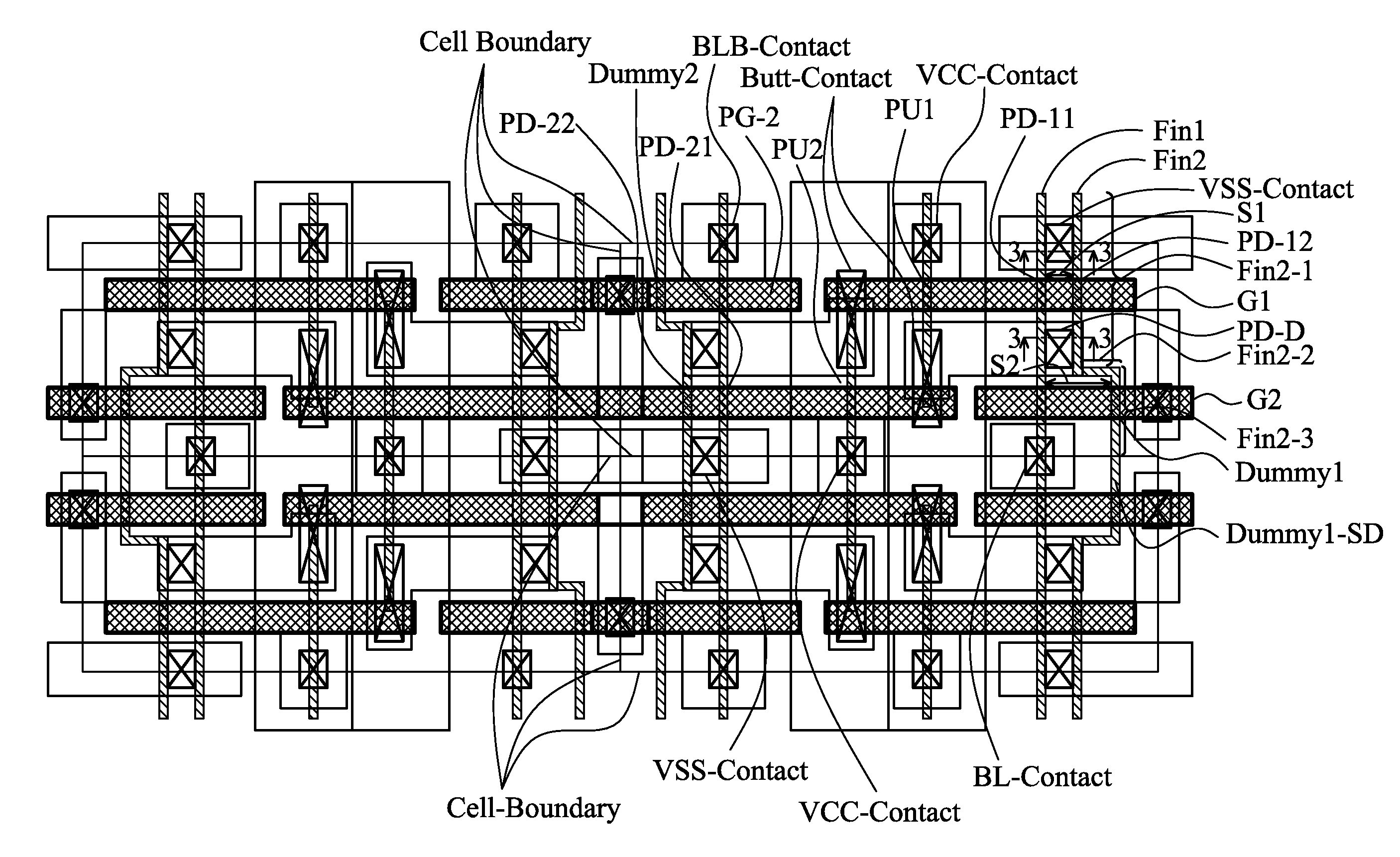
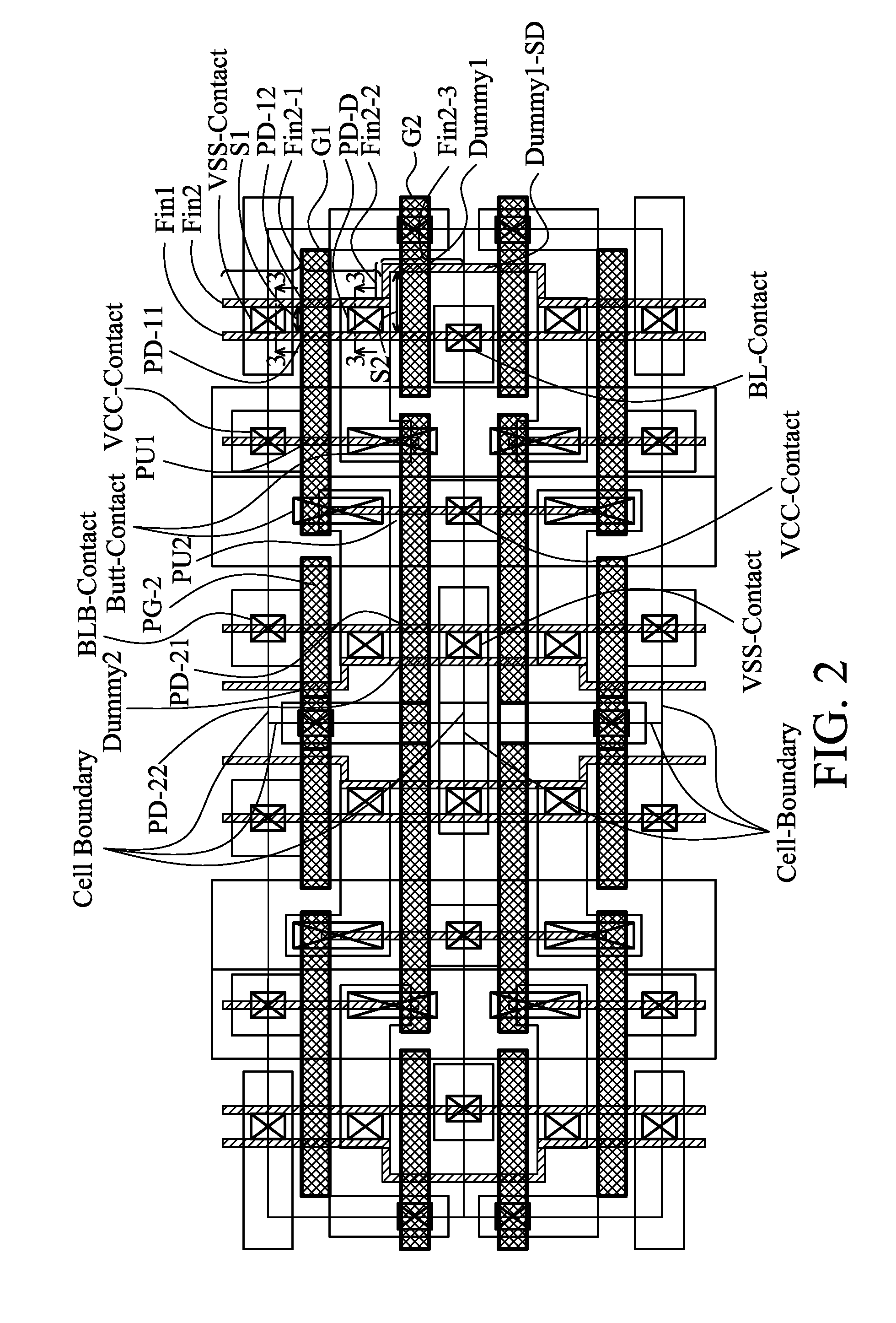
A novel static random access memory (SRAM) comprising multi-fin Fin field-effect transistors (FinFETs) and the corresponding layouts are presented. The variations of the embodiment are then discussed. Throughout the various views and illustrative embodiments, like reference numbers are used to designate like elements.

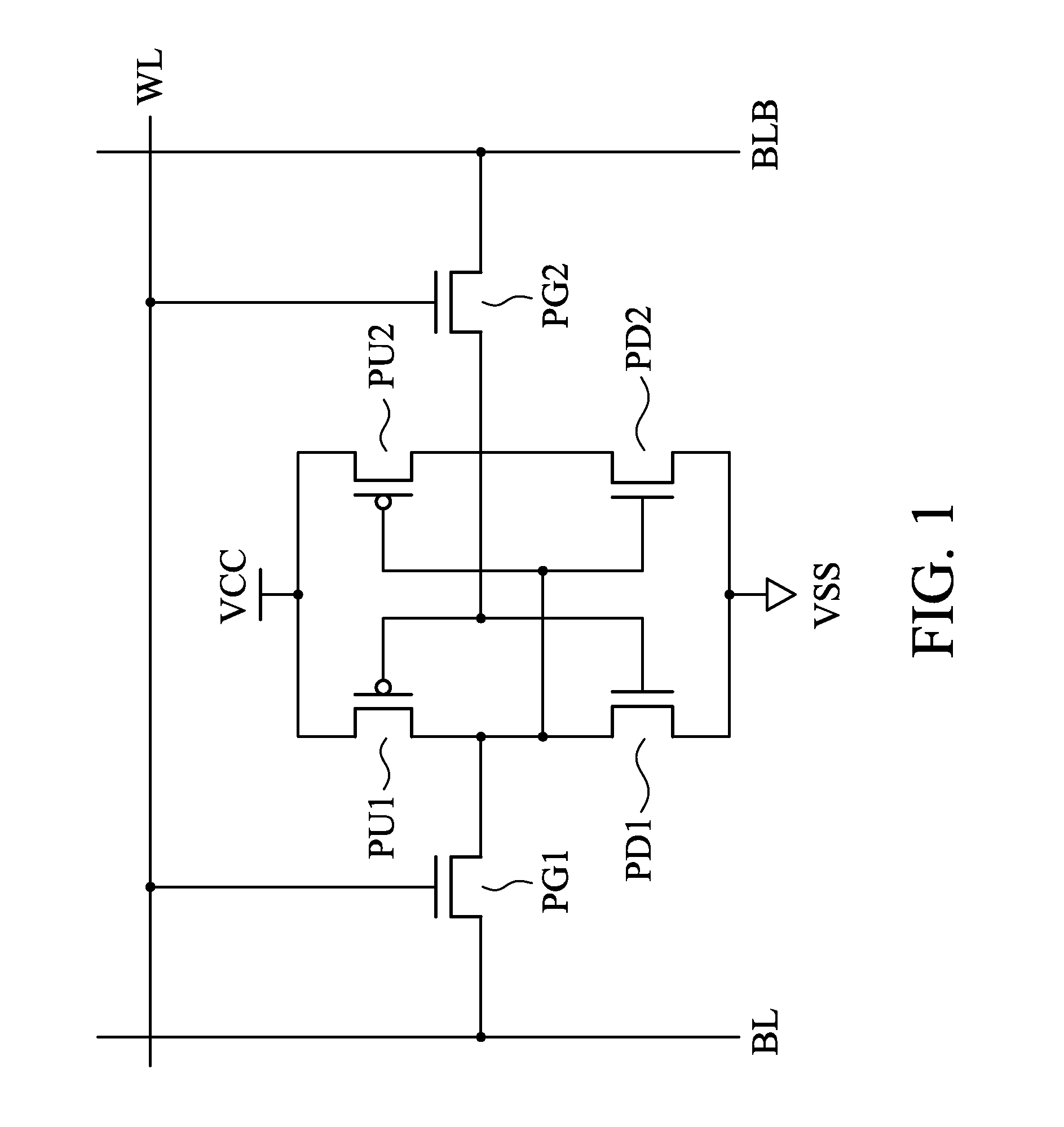
FIG. 1 illustrates a circuit diagram of an SRAM cell in accordance with an embodiment. The SRAM cell includes pass-gate transistors PG1 and PG2, pull-up transistors PU1 and PU2, and pull-down transistors PD1 and PD2. The gates of pass-gate transistors PG1 and PG2 are control...


PUM


Abstract

A static random access memory (SRAM) cell includes a straight fin and a bended fin physically disconnected from the straight fin. The bended fin has a first portion and a second portion parallel to the straight fin. The distance between the first portion of the bended fin and the straight fin is smaller than the distance between the second portion of the bended fin and the straight fin. The SRAM cell includes a pull-down transistor including a portion of a first gate strip, which forms a first and a second sub pull-down transistor with the straight fin and the first portion of the bended fin, respectively. The SRAM cell further includes a pass-gate transistor including a portion of a second gate strip, which forms a first sub pass-gate transistor with the straight fin. The pull-down transistor includes more fins than the pass-gate transistor.

Description

TECHNICAL FIELDThis disclosure relates generally to integrated circuit devices, and more particularly to memory cells, and even more particularly to layout design and manufacturing methods of static random access memory (SRAM) cells comprising FinFETs.BACKGROUNDFin field-effect transistors (FinFETs) are widely used in integrated circuits for their increased gate widths over planar transistors. A major advantageous feature of the FinFETs is that they use small chip areas. To maximize this benefit, when used in high-density devices, for example, static random access memory (SRAM) arrays, the FinFETs were often designed as single-fin FinFETs.The SRAMs with single-fin FinFETs, however, often suffer from low cell ratio problems such as low beta ratios. The beta ratios are the ratios of the drive currents of pull-down transistors to the drive currents of the respective pass-gate transistors. The beta ratios are important for the cell stability. Generally, the beta ratios are preferably gr...

Claims


Application Information

Patent Timeline
IPC IPC(8): H01L27/11
CPCH01L27/0207H01L29/785H01L27/1104H01L27/11H01L29/41791H10B10/00H10B10/12
Inventor LIAW, JHON-JHY
Owner TAIWAN SEMICON MFG CO LTD
Why Eureka
Try Eureka