
Bifacial solar cell

Inactive Publication Date: 2011-06-16
IND TECH RES INST
View PDF18 Cites 23 Cited by
  • Summary
  • Abstract
  • Description
  • Claims
  • Application Information

AI Technical Summary

Benefits of technology

[0010]The present invention is directed to a bifacial solar cell, which could reduce the carrier recombination on the surface and increase cell efficiency.
[0014]According to the bifacial solar cell of the present invention, a fixed charge layer is added between a rear surface of a substrate and an anti-reflection coating layer, which can prevent recombination of carriers on the rear surface and improve cell efficiency.

Problems solved by technology

In recent years, the environmental problems are highly concerned.
However, since such type of the solar cell uses opaque metal as the rear surface electrode, only a single side thereof can absorb the sunlight.
Therefore, such type of the solar cell is not suitable for a bifacial type building integrated photovoltaic (BIPV) serving as a curtain wall.
Presently, in a HIT solar cell disclosed by a Japan Sanyo company, a plasma enhanced chemical vapor deposition (PECVD) process is used to fabricate a PN junction at a positive electrode, and a BSF structure is also fabricated on the rear surface according to the PECVD process, though a fabrication process thereof is greatly different to that of a conventional solar cell, and a fabrication equipment thereof is expensive.

Method used


Image

  • Bifacial solar cell
  • Bifacial solar cell
  • Bifacial solar cell

Examples


Embodiment Construction

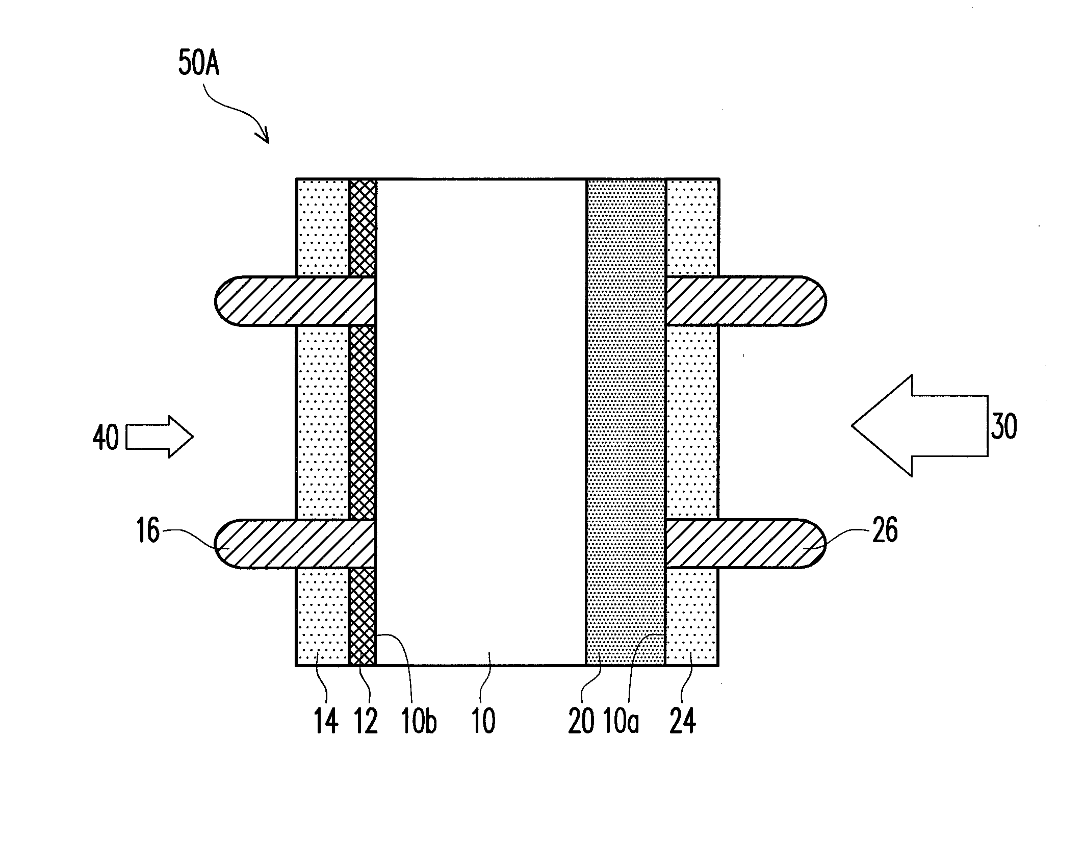
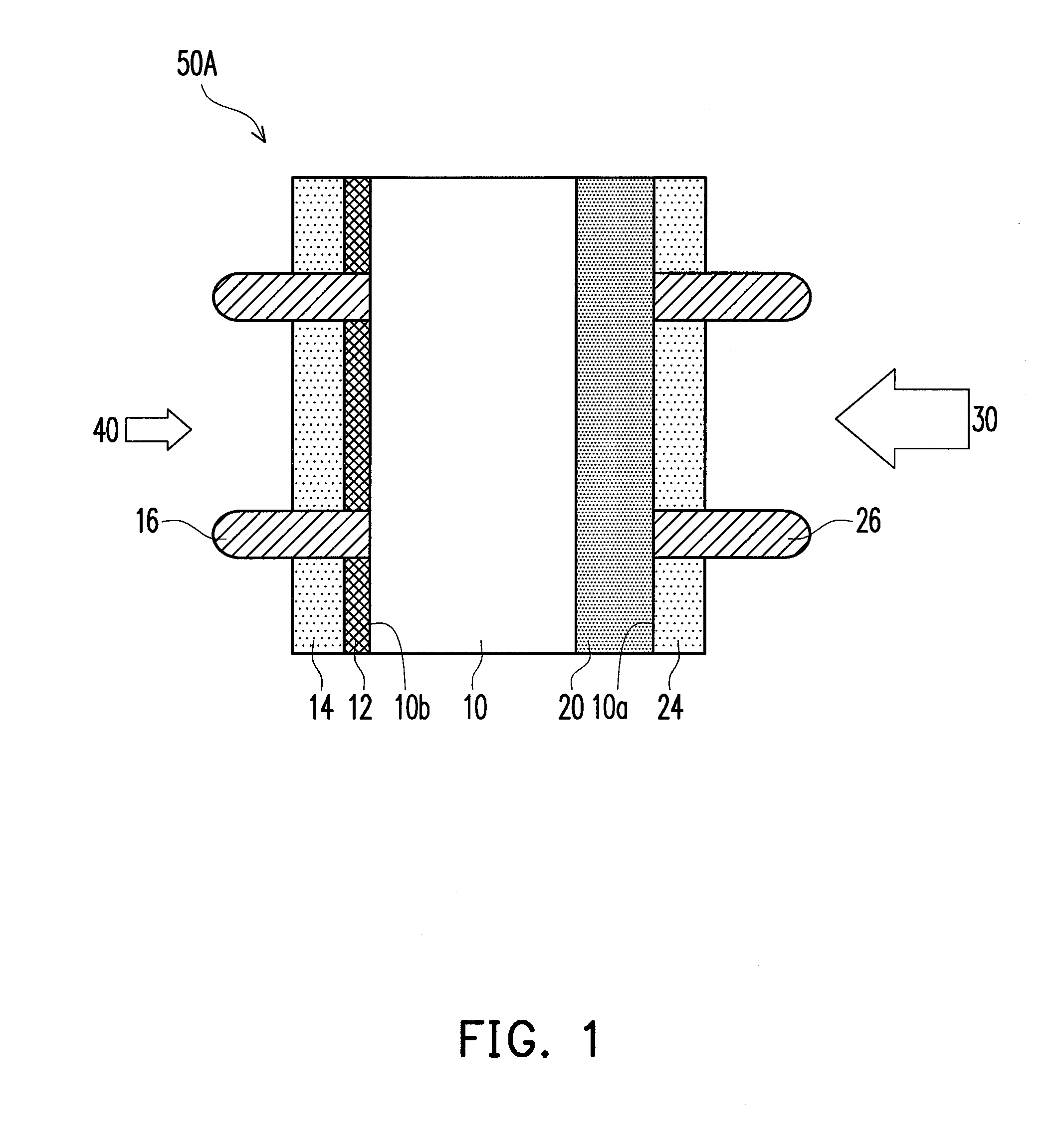
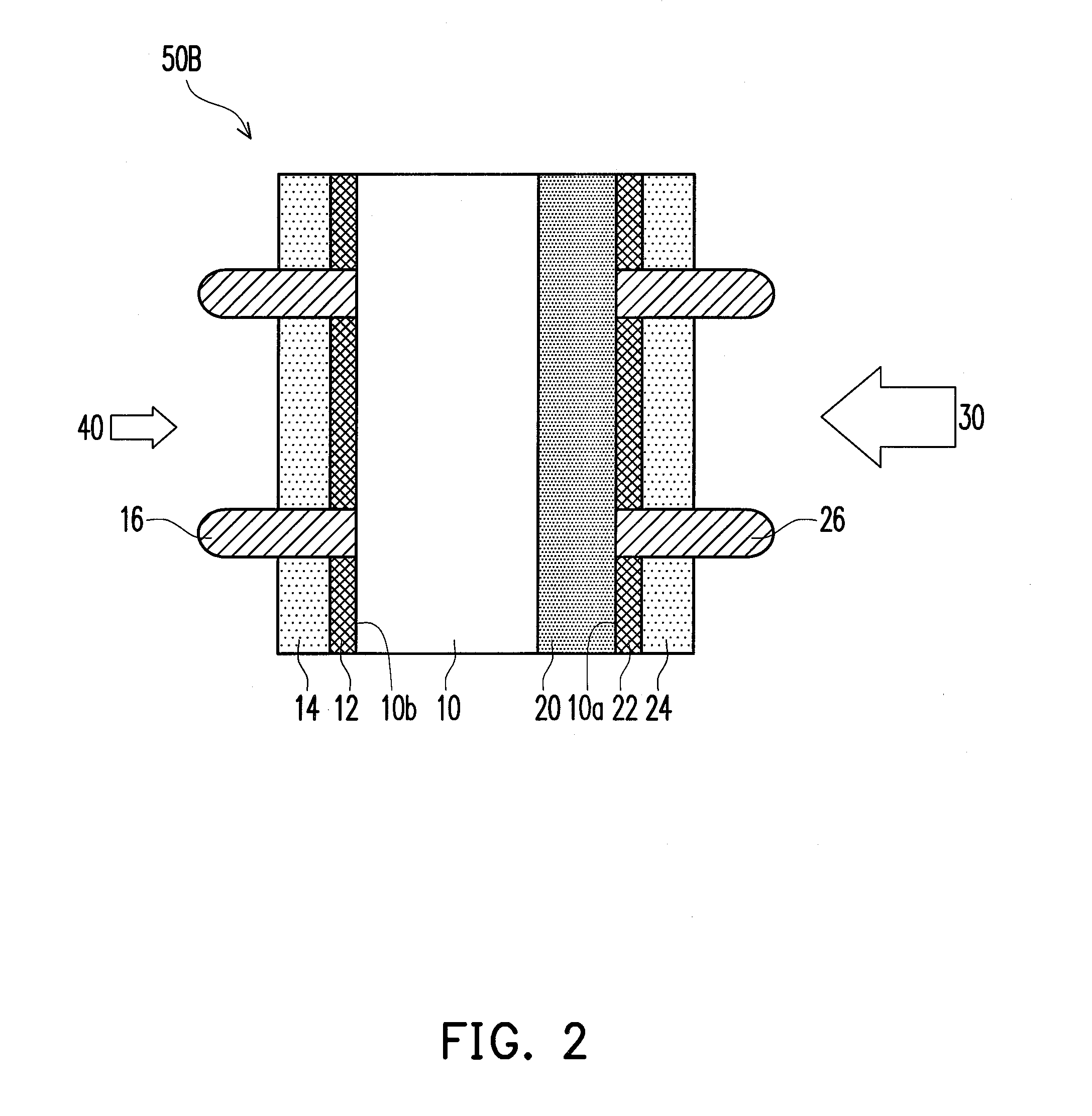
[0022]FIG. 1 is a cross-sectional view of a bifacial solar cell according to an embodiment of the present invention. FIG. 2 is a cross-sectional view of another bifacial solar cell according to an embodiment of the present invention. For simplicity's sake, the same numerals are used in the drawings and the description to refer to the same or like parts.

[0023]Referring to FIG. 1, the bifacial solar cell 50A includes a semiconductor substrate 10, a fixed charge layer 12, an anti-reflection coating layer 14, an electrode 16, a semiconductor layer 20, an anti-reflection coating layer 24 and an electrode 26.

[0024]Referring to FIG. 2, the bifacial solar cell 50B includes a semiconductor substrate 10, a fixed charge layer 12, an anti-reflection coating layer 14, an electrode 16, a semiconductor layer 20, a fixed charge layer 22, an anti-reflection coating layer 24 and an electrode 26.

[0025]The semiconductor substrate 10 is of a first conductive type, and the semiconductor layer 20 is of a ...


PUM


Abstract

A bifacial solar cell including a semiconductor substrate of a first conductivity type, a fixed charge layer, a first grid electrode, a semiconductor layer of a second conductivity type and a second grid electrode are provided. The fixed charge layer is located on a rear surface of the semiconductor substrate. The first grid electrode is located over the rear surface of the semiconductor substrate and electrically connected to the rear surface of the semiconductor substrate by penetrating through the fixed charge layer. The semiconductor layer is located on the front surface of the semiconductor layer. The second grid electrode is located over and electrically connected to the semiconductor layer.

Description

CROSS-REFERENCE TO RELATED APPLICATION[0001]This application claims the priority benefit of Taiwan application serial no. 98142752, filed on Dec. 14, 2009. The entirety of the above-mentioned patent application is hereby incorporated by reference herein and made a part of this specification.BACKGROUND OF THE INVENTION[0002]1. Field of the Invention[0003]The present invention relates to a bifacial solar cell.[0004]2. Description of Related Art[0005]In recent years, the environmental problems are highly concerned. To resolve a problem of energy shortage and reduce an impact on the environment caused by using the fossil energy, research of alternative energy and renewable energy become an important topic. Since a solar cell can directly convert solar energy into electric power, and none greenhouse gases such as carbon dioxide is produced during the power generation process, the solar cell becomes a focus of attention.[0006]A crystalline silicon solar cell is a kind of most popular sola...

Claims


Application Information

Patent Timeline
IPC IPC(8): H01L31/00
CPCH01L31/02167Y02E10/547H01L31/068H01L31/022433
Inventor DU, CHEN-HSUNSUN, WEN-CHINGCHANG, WEI-LUN
Owner IND TECH RES INST
Learn More