Three-dimensional CMOS circuit on two offset substrates and method for making same

a cmos circuit and offset substrate technology, applied in the direction of resistors, electrical devices, solid-state devices, etc., can solve the problems of complex integration, high cost, and limited application of the approach, and achieve the effects of compactness, easy production, and economical

Inactive Publication Date: 2011-06-16
COMMISSARIAT A LENERGIE ATOMIQUE ET AUX ENERGIES ALTERNATIVES
View PDF25 Cites 3 Cited by
  • Summary
  • Abstract
  • Description
  • Claims
  • Application Information

AI Technical Summary

Benefits of technology

[0007]The object of the invention is to provide a circuit that is easy to produce, is compact, economical and presents high-speed devices.

Problems solved by technology

However, this approach reveals to be very limited in its application as the gain in mobility is not sufficient for both types of carriers at the same time.
However, this integration is complex and costly as the integrated circuit is not very compact and it is necessary to work with different substrates which is delicate to manage in a production line.

Method used


Image

  • Three-dimensional CMOS circuit on two offset substrates and method for making same
  • Three-dimensional CMOS circuit on two offset substrates and method for making same
  • Three-dimensional CMOS circuit on two offset substrates and method for making same

Examples


Embodiment Construction

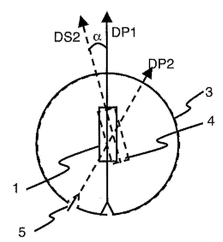
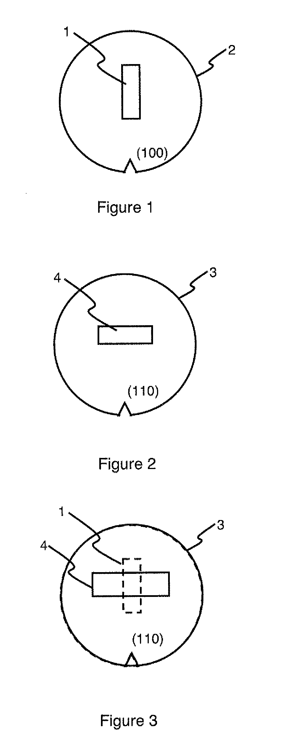
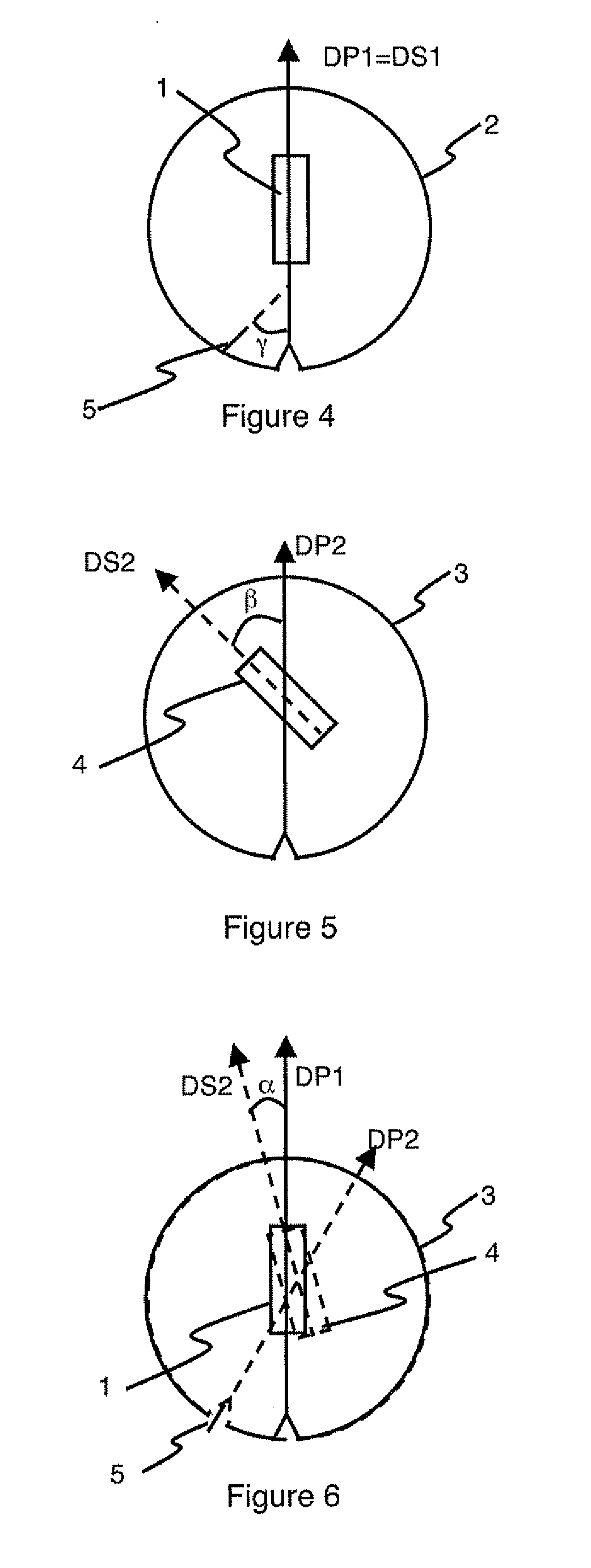
[0013]As illustrated in FIG. 4, first field-effect transistors 1 are produced on a first crystalline substrate 2 which comprises a main crystallographic direction DP1. First transistors 1 are oriented along a first secondary crystallographic direction DS1. This orientation can be materialized by the longitudinal axis of the gate electrode or by the axis joining the source and drain of the transistor.

[0014]in conventional manner, the main crystallographic direction of a crystalline substrate is materialized by a notch or by a flat. Conventionally in microelectronics, the main crystallographic direction is the direction. However crystalline substrates also exist which have a main crystallographic direction of type or another direction.

[0015]The surface of first substrate 2 is furthermore a plane which is advantageous for the electronic characteristics of first transistors 1. The surface of first substrate 2 can for example be a (100) plane or a (110) plane.

[0016]The notch or flat wh...


PUM


Abstract

A three-dimensional CMOS circuit having at least a first N-conductivity field-effect transistor and a second P-conductivity field-effect transistor respectively formed on first and second crystalline substrates. The first field-effect transistor is oriented, in the first substrate, with a first secondary crystallographic orientation. The second field-effect transistor is oriented, in the second substrate, with a second secondary crystallographic orientation. The orientations of the first and second transistors form a different angle from the angle formed, in one of the substrates, by the first and second secondary crystallographic directions. The first and second substrates are assembled vertically.

Description

BACKGROUND OF THE INVENTION[0001]The invention relates to a three-dimensional CMOS circuit comprising at least first field-effect transistors of a first conductivity type and second field-effect transistors of a second conductivity type respectively formed on first and second crystalline substrates, the first and second substrates being assembled vertically.[0002]The invention also relates to a method for three-dimensional co-integration of a CMOS circuit successively comprising production of first field-effect transistors of a first conductivity type on a first substrate, bonding of a second substrate covering the first transistors and production of second field-effect transistors of a second conductivity type on the second substrate.STATE OF THE ART[0003]Seeking to achieve rapidity in C-MOS integrated circuits implies a reduction of the transistor switching times and of the propagation delays in the circuit interconnections.[0004]Reduced switching times can be obtained by reducing...

Claims


Application Information

Patent Timeline
Patent Type & Authority Applications(United States)
IPC IPC(8): H01L27/092H01L21/336
CPCH01L21/8221H01L21/823807H01L29/045H01L27/092H01L27/0688
Inventor VINCENT, BENJAMIN
Owner COMMISSARIAT A LENERGIE ATOMIQUE ET AUX ENERGIES ALTERNATIVES
Why Eureka
Try Eureka