

Semiconductor device and fabrication method for the same
a technology of semiconductor devices and semiconductors, applied in semiconductor devices, diodes, electrical devices, etc., can solve the problems of switching power loss, on-state power loss, and reduced resistance of mosfet, so as to reduce the reverse recovery time trr
- Summary
- Abstract
- Description
- Claims
- Application Information
AI Technical Summary
Benefits of technology
Problems solved by technology
Method used
Image

Examples
first embodiment
Element Structure
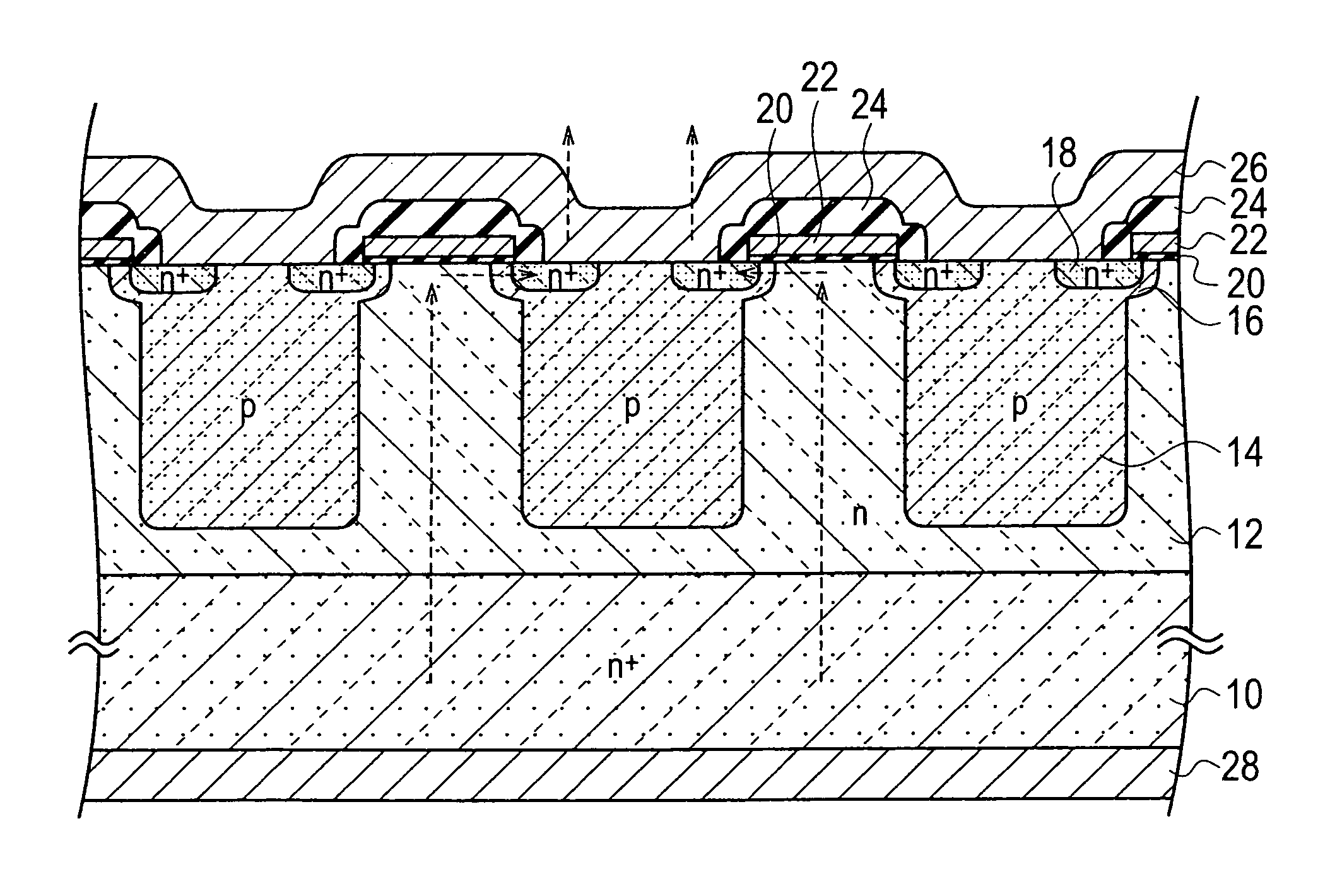
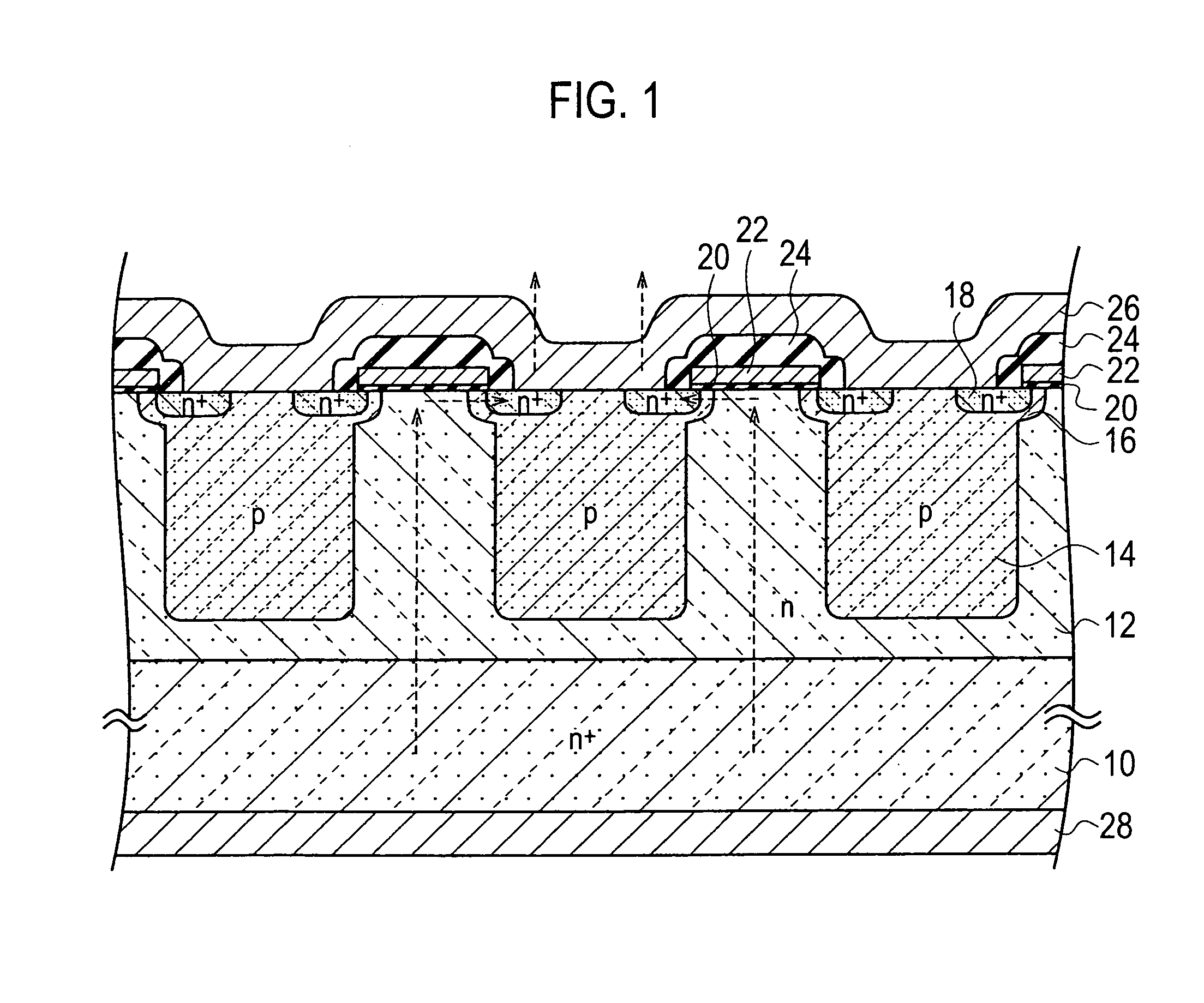
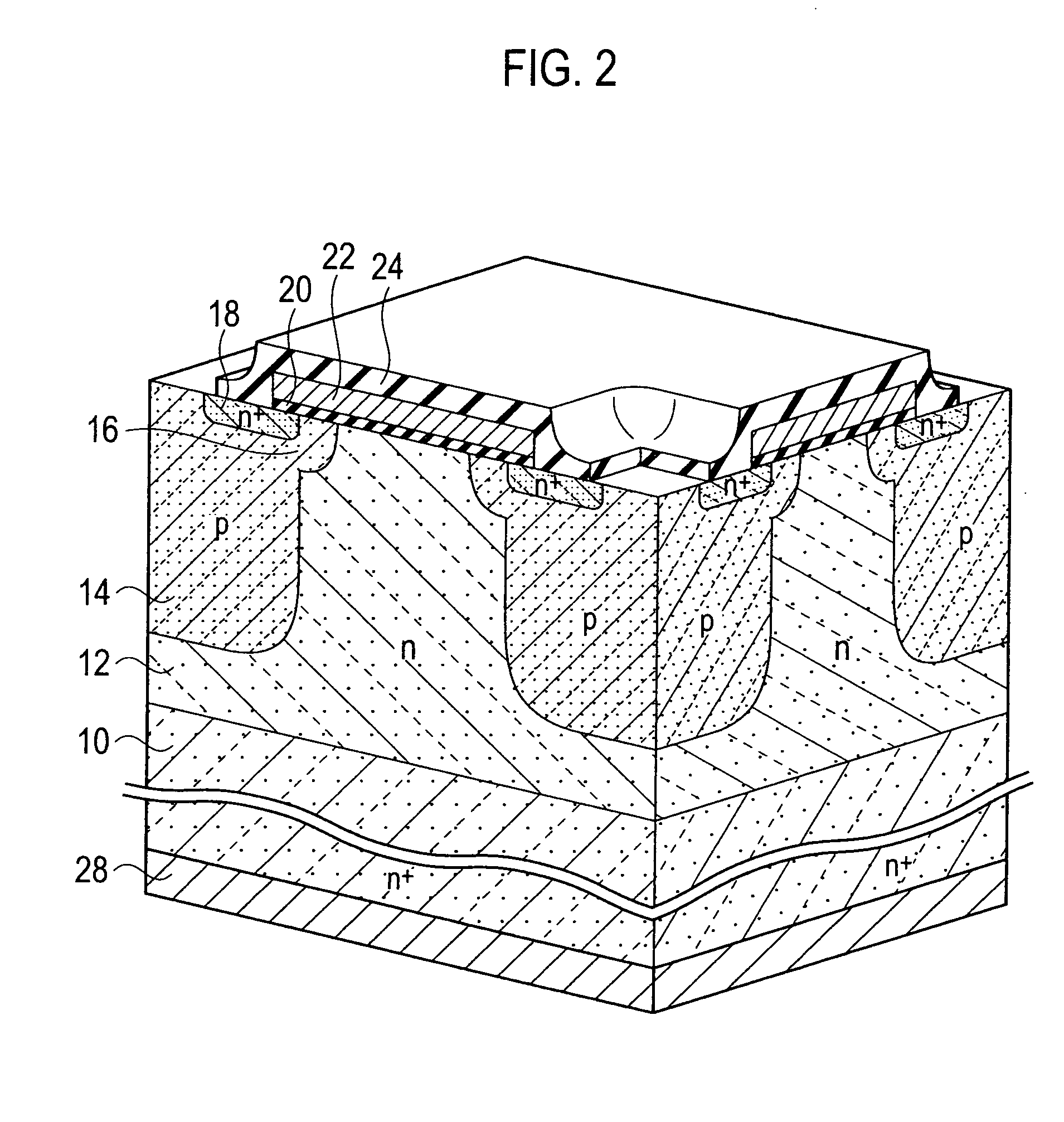
[0033]FIG. 1 shows a schematic cross-section structure of a semiconductor device according to a first embodiment of the present invention. Moreover, FIG. 2 shows a schematic bird's-eye view structure of the semiconductor device according to the first embodiment.
[0034]As shown in FIG. 1 to FIG. 2, the semiconductor device according to the first embodiment includes: an n type impurity doped high resistivity first base layer 12; an n type impurity doped drain layer 10 disposed on the back side surface of the first base layer 12; a p type impurity doped second base layer 16 formed on the surface of the first base layer 12; an n type impurity doped source layer 18 formed on the surface of the second base layer 16; a gate insulating film 20 disposed on the surface of both the source layer 18 and the second base layer 16; a gate electrode 22 disposed on the gate insulating film 20; a p type impurity doped column layer 14 formed in the first base layer 12 of the lower part ...
PUM
 Abstract
Description
Claims
Application Information