Optical Proximity Correction for Improved Electrical Characteristics

a technology of optical proximity and electrical characteristics, applied in the field of computer-aided design of photolithographic masks, can solve the problems of reducing the fidelity of the image projected onto the photoresist, and not necessarily optimal electrical behavior obtained from such techniques, so as to improve optical proximity correction, improve the electrical properties of the device, and minimize the effect of edge placement error

Inactive Publication Date: 2011-06-23
IBM CORP
View PDF31 Cites 7 Cited by
  • Summary
  • Abstract
  • Description
  • Claims
  • Application Information

AI Technical Summary

Benefits of technology

[0010]Accordingly, the present invention provides a method, computer program product, and data processing system for performing an improved optical proximity correction that better respects the electrical properties of the device being manufactured. Specifically, the present invention recognizes that the electrical properties of a given device are a function of its dimensions (size), as opposed to its edge positions (shape). In particular, a preferred embodiment of the present invention performs OPC by first dividing the perimeter of a mask region in an integrated circuit into a plurality of segments, then grouping the segments into at least two distinct groups, wherein segm

Problems solved by technology

The minimum feature sizes available in a given technology are limited, at least in part, by the nature of the photolithographic process itself.
Specifically, as feature sizes approach the wavelengths of light used in the process (e.g., at sub-micron feature sizes for conventional photolithography using ultraviolet light), diffraction (a result of the wave-nature of electromagnetic radiation) reduces the fidelity of the image projected onto the ph

Method used


Image

  • Optical Proximity Correction for Improved Electrical Characteristics
  • Optical Proximity Correction for Improved Electrical Characteristics
  • Optical Proximity Correction for Improved Electrical Characteristics

Examples


Embodiment Construction

[0021]The following is intended to provide a detailed description of an example of the invention and should not be taken to be limiting of the invention itself. Rather, any number of variations may fall within the scope of the invention, which is defined in the claims following the description.

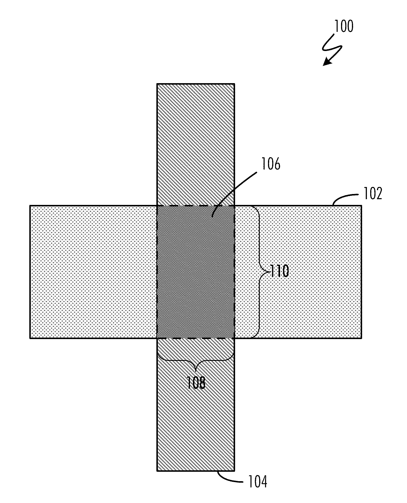
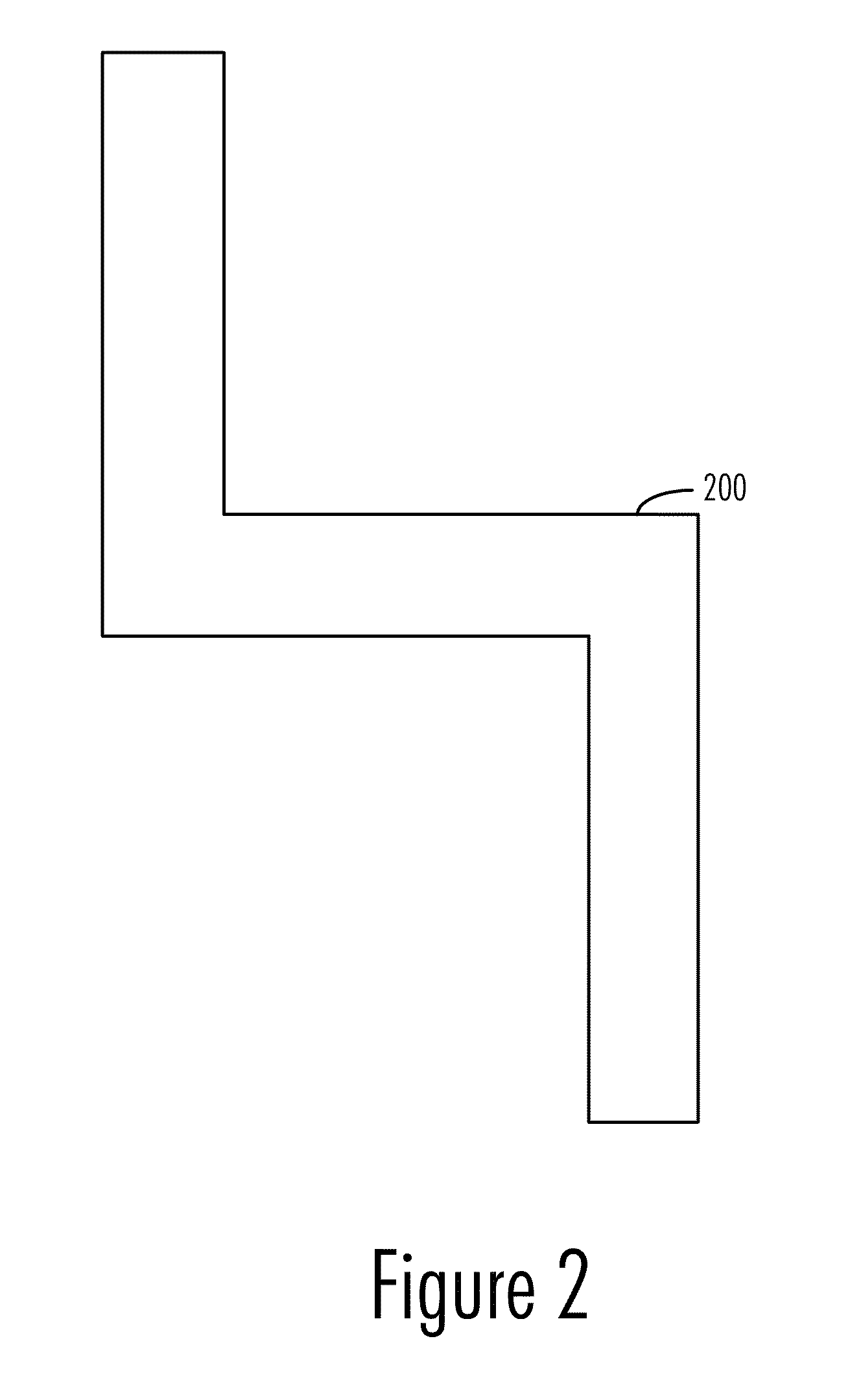
[0022]Operation of a preferred embodiment of the present invention is illustrated with respect to an exemplary feature or “region”502 in a photomask pattern. For the purpose of this example, a purely rectangular region is selected, which would be representative of a simple polysilicon layer utilized to form the gate of a single MOSFET, such as MOSFET 100 in FIG. 1. The process of performing optical proximity correction in this preferred embodiment of the invention begins with the division of the perimeter of region 502 into a plurality of segments, such as segment 504. These segments are then grouped into two groups, shown here as group 506 and group 508. One of these groups (we will choose gr...


PUM


Abstract

A method, computer program product, and data processing system for performing an improved optical proximity correction are disclosed, which better respect the electrical properties of the device being manufactured. A preferred embodiment of the present invention performs OPC by first dividing the perimeter of a mask region into a plurality of segments, then grouping the segments into at least two distinct groups, wherein segments in the first of these groups are adjusted in position so as to minimize edge placement error (EPE) when the photolithography using the mask is simulated. Segments in the second group are adjusted in position so as to minimize cumulative error in a dimension spanning the region, wherein the span of such dimension extends from segments in the first group to segments in the second group. Correction so obtained by this process more readily preserves the intended electrical behavior of the original device design.

Description

BACKGROUND OF THE INVENTION[0001]1. Technical Field[0002]The present invention relates generally to computer-aided design of photolithographic masks used in the manufacturing of integrated circuits. More specifically, the present invention is directed to an improved method, computer program product, and apparatus for performing optical proximity correction in such masks.[0003]2. Description of the Related Art[0004]Integrated circuits (ICs) are commonly manufactured through a photolithographic process. In photolithography, a layer of light-sensitive material (photoresist) is applied atop a layer of material to be etched by the process. A geometric pattern is applied to the photoresist by shining light of a prescribed wavelength through a photolithographic mask (also referred to as a “photomask” or, simply, “mask”) containing the pattern. A photomask is an opaque plate with holes or transparencies that allow light to shine through in a defined pattern. (Henceforth herein, the term “re...

Claims


Application Information

Patent Timeline
IPC IPC(8): G06F17/50
CPCG03F1/36G03F1/144
Inventor AGARWAL, KANAK B.NASSIF, SANI R.
Owner IBM CORP
Why Eureka
Try Eureka