Image sensor packaging structure with low transmittance encapsulant

a technology of low transmittance encapsulation and image sensor, which is applied in the direction of basic electric elements, electrical apparatus, and semiconductor devices, etc., can solve the problems of increasing the complexity of the fabrication process of the image sensor packaging structure and incurring costs of 14

Active Publication Date: 2011-06-30
TONG HSING ELECTRONICS INDS
View PDF6 Cites 114 Cited by
  • Summary
  • Abstract
  • Description
  • Claims
  • Application Information

AI Technical Summary

Benefits of technology

[0009]The present invention relates to an image sensor packaging structure with a low transmittance encapsulant for encapsulating the image senso...

Problems solved by technology

Although the housing 14 blocks ambient light and thereby improves image sensing quality, not only does alignment of the housing 14 pose a...

Method used


Image

  • Image sensor packaging structure with low transmittance encapsulant
  • Image sensor packaging structure with low transmittance encapsulant
  • Image sensor packaging structure with low transmittance encapsulant

Examples


Embodiment Construction

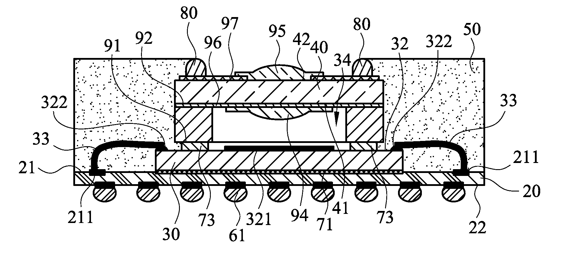
[0031]Referring to FIG. 2A, in this embodiment, an image sensor packaging structure with a low transmittance encapsulant includes a substrate 20, a chip 30, a transparent lid 40, and a low transmittance encapsulant 50.

[0032]Referring to FIG. 2A, the substrate 20 is configured for general use with an image sensor packaging structure. For instance, the substrate 20 is a circuit board with a circuit structure. The substrate 20 has a carrying surface 21 and a bottom surface 22. The carrying surface 21 is the upper surface of the substrate 20. The bottom surface 22 is the lower surface of the substrate 20. A plurality of first conductive contacts 211 is disposed on the carrying surface 21 of the substrate 20. A plurality of solder balls 61 is implanted on the bottom surface 22 of the substrate 20.

[0033]The substrate 20 is provided with a circuit structure. The circuit structure allows the first conductive contacts 211 and the solder balls 61 to be signal-connected. Hence, the image senso...


PUM


Abstract

An image sensor packaging structure with a low transmittance encapsulant is provided. The image sensor packaging structure includes a substrate, a chip, a transparent lid, and the low transmittance encapsulant. The chip is combined with the substrate. The transparent lid is adhered to the chip and cover above a sensitization area of the chip to form an air cavity. The low transmittance encapsulant is formed on the substrate and encapsulates the chip and the transparent lid so as to accomplish the package of the image sensor packaging structure. Due to the feature of prohibiting from light passing through the low transmittance encapsulant, the arrangement of the low transmittance encapsulant can avoid the light from outside interfere the image sensing effect of the image sensor. Therefore, the quality of the image sensing can be ensured.

Description

BACKGROUND OF THE INVENTION[0001]1. Field of the Invention[0002]The present invention relates to image sensor packaging structures with low transmittance encapsulants, and more particularly, to an image sensor packaging structure for use in improving the image sensing quality.[0003]2. Description of the Prior Art[0004]The advent and prevalence of various digital video products are followed by ever-increasing demand for image sensors for use with digital video products, such as digital still cameras, cell phone cameras, and video phones. Image sensors work by converting received optical signals into electrical signals and then analyzing the electrical signals by an external device. Hence, image sensors can be integrated into electronic products to perform related imaging functions, such as taking pictures and shooting videos.[0005]FIG. 1A is a disassembled schematic view of a conventional image sensor packaging structure 10. FIG. 1B is an assembled schematic view of FIG. 1A.[0006]Ref...

Claims


Application Information

Patent Timeline
IPC IPC(8): H01L31/0232
CPCH01L2224/97H01L27/14683H01L2224/48091H01L24/32H01L2924/15311H01L24/73H01L2224/48471H01L2924/16235H01L24/97H01L2224/73265H01L27/14618H01L27/14625H01L2224/49175H01L27/14623H01L2224/32225H01L2224/48479H01L24/48H01L2924/1815H01L2224/48227H01L2924/00014H01L2224/45099H01L2924/00H01L24/49H01L2224/4554
Inventor TU, HSIU-WENHSIN, CHUNG-HSIENCHUANG, CHUN-HUAKUO, REN-LONGLIN, CHIN-FUSHIAO, YOUNG-HOUNG
Owner TONG HSING ELECTRONICS INDS
Why Eureka
Try Eureka