

Electroluminescence device
- Summary
- Abstract
- Description
- Claims
- Application Information
AI Technical Summary
Benefits of technology
Problems solved by technology
Method used
Image

Examples
Embodiment Construction
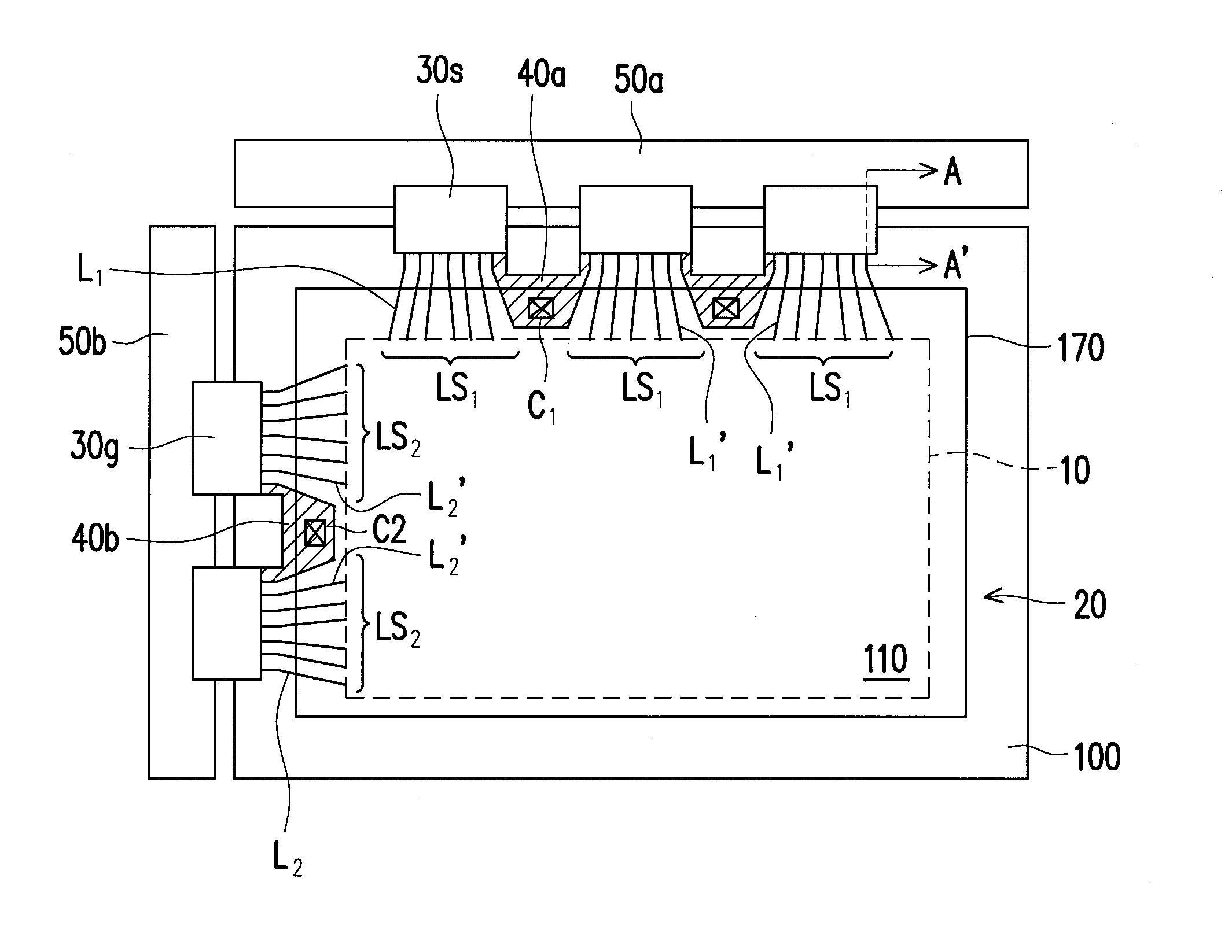
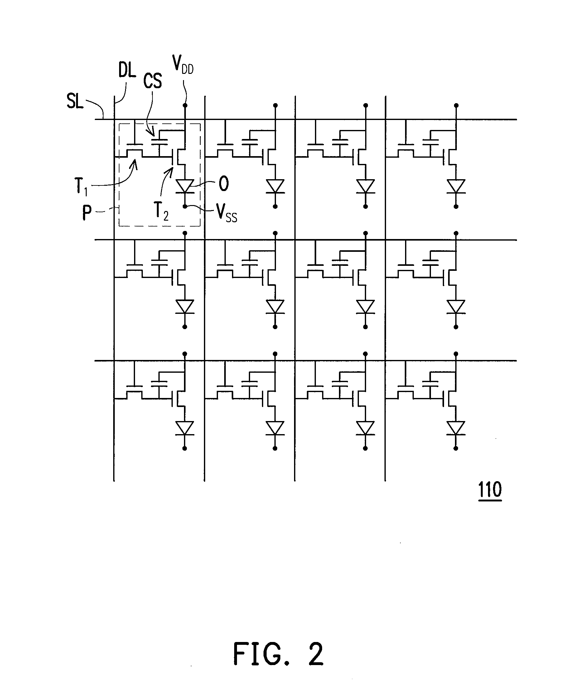
[0018]FIG. 1 is a top view of an electroluminescence device according to one embodiment of the present invention. FIG. 2 illustrates an equivalent circuit of the pixel array of the electroluminescence device of FIG. 1. FIG. 3 is a partial view of the peripheral circuit region of FIG. 1. FIG. 4 is a cross-sectional view of one pixel structure of the pixel array of FIG. 2.
[0019]Referring first to FIG. 1, the electroluminescence device of the present embodiment includes a substrate 100, a pixel array 110, a plurality of lead line sets LS, a plurality of driving devices 30s, 30g, and at least one power transmission pattern 40a, 40b.
[0020]The substrate 100 includes a display region 10 and a peripheral circuit region 20 around the display region 10. The substrate 100 may be a transparent substrate such as a transparent glass substrate or a transparent flexible substrate. The substrate 100 is mainly used to support components of the electroluminescence device. In order to enable the light...
PUM
 Abstract
Description
Claims
Application Information