Semiconductor optical element and integrated semiconductor optical element

a semiconductor optical element and semiconductor technology, applied in semiconductor lasers, laser details, electrical apparatus, etc., can solve the problems of reducing efficiency, deteriorating reducing efficiency, so as to achieve high speed response characteristics, high barrier to electrons, and high speed response characteristics.

Active Publication Date: 2011-06-30
MITSUBISHI ELECTRIC CORP
View PDF5 Cites 5 Cited by
  • Summary
  • Abstract
  • Description
  • Claims
  • Application Information

AI Technical Summary

Benefits of technology

[0032]According to the present invention, the Fe-doped semiconductor layer formed in the buried layer of the semiconductor optical element is not grown on the (111)B surface of the crystal plane formed by the first p-type semiconductor layer and the first n-type semiconductor layer, and the second n-type semiconductor layer formed in the buried layer is not grown on the (111)B surface of the crystal plane formed by the first p-type semiconductor layer, the first n-type semiconductor layer, and the Fe-doped semiconductor layer. This prevents Zn as a dopant in the first p-type semiconductor layer and the second p-type semiconductor layer from diffusing from the first p-type semiconductor layer and the second p-type semiconductor layer into the Fe-doped semiconductor layer.
[0033]Further, according to the present invention, the low carrier concentration semiconductor layer formed in the buried layer of the semiconductor optical element is not grown on the (111)B surface of the crystal plane formed by the first p-type semiconductor layer and the first n-type semiconductor layer. This makes it possible to form the semiconductor optical element without consideration of interdiffusion.
[0034]Therefore, a semiconductor optical element which may suppress a reactive current flow through the buried layer and may materialize high speed response characteristics may be obtained.
[0035]Further, according to the present invention, in the integrated semiconductor optical element, as the lowermost layer of the regrown semiconductor layer formed on the side portion of the semiconductor optical element having the mesa-stripe-shaped laminate formed therein, one of an AlInAs layer and an AlGaInAs layer of one of p-type and low carrier concentration is laminated. By using one of an AlInAs layer and an AlGaInAs layer which has a high barrier to electrons, an integrated semiconductor optical element which may suppress the reactive current and may materialize the high speed response characteristics may be obtained.

Problems solved by technology

In this case, as illustrated in FIG. 10A, leakage current paths which is irrelevant to action of the semiconductor optical element are formed in the buried layers, and thus, there are problems that reactive current increases to decrease the efficiency and the high speed response characteristics are deteriorated.
When the Fe-doped semiconductor layer 57 is grown so as not to be in contact with a p-type semiconductor layer, as illustrated in FIGS. 10B and 10C, there is a problem that, because there are the plurality of n-type semiconductor layers, reactive current increases to decrease the efficiency.
More specifically, in a semiconductor optical element in which an Fe-doped semiconductor layer is used as a buried layer, there are problems that, due to interdiffusion between Fe and Zn and the like, reactive current increases to decrease the efficiency and the high speed response characteristics are deteriorated.
However, because crystal growth conditions of an Ru-doped semiconductor layer for obtaining a satisfactory surface state as that of an Fe-doped semiconductor layer are very strict, an Ru-doped semiconductor layer lacks stability, and it is known that this tendency is conspicuous particularly when the Ru-doped semiconductor layer is thick.
Further, because the crystal growth conditions are strict, it may be difficult to obtain a high activation rate and a high resistivity.
Therefore, there is a problem that it may be difficult to, in order to decrease the parasitic capacitance and to materialize high speed response characteristics, grow a thick Ru-doped semiconductor layer and to exert a current blocking function only by the Ru-doped semiconductor layer.
However, such conventional art has the following problems.
Therefore, in this case, because the low carrier concentration semiconductor layer exhibits properties of a weak n-type semiconductor, as illustrated in FIG. 11, leakage current paths are formed in the buried layers, and thus, there is a problem that reactive current increases to decrease the efficiency.
Further, when the low carrier concentration semiconductor layer is grown so as to be thin in order to suppress a reactive current flow through the buried layers, there is a problem that the parasitic capacitance of the buried layers increases to deteriorate the high speed response characteristics.
Because the structure of an integrated semiconductor optical element is complicated, to suppress the reactive current therein is difficult in many cases.
Further, because, in an integrated semiconductor optical element, semiconductor regions having different functions from one another and integrated so as to be adjacent to one another have structures different from one another, and the structures may not be greatly changed, to suppress leakage current to the integrated semiconductor regions is difficult in many cases.
In particular, when the upper cladding layer of the semiconductor laser portion is an n-type semiconductor, it is difficult to suppress the leakage current.

Method used


Image

  • Semiconductor optical element and integrated semiconductor optical element
  • Semiconductor optical element and integrated semiconductor optical element
  • Semiconductor optical element and integrated semiconductor optical element

Examples


embodiment 1

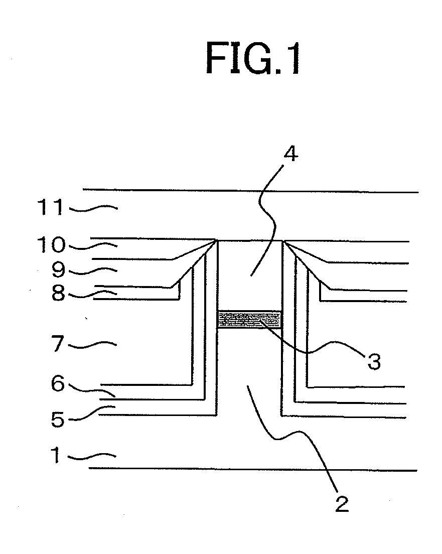
[0050]FIG. 1 is a sectional view illustrating a structure of a semiconductor optical element according to Embodiment 1 of the present invention. Here, as an example of the semiconductor optical element, a distributed-feedback semiconductor laser is described.

[0051]In FIG. 1, a p-type cladding InP layer 2, an active layer 3, and an n-type cladding InP layer 4 are laminated in the stated order from the bottom on an InP substrate 1 to form a mesa-stripe-shaped laminate. A buried layer is formed on each side of the laminate. In the buried layer, a first p-type InP layer 5, a first n-type InP layer 6, an Fe-doped semiconductor layer 7, a second n-type InP layer 8, an undoped 1-type InP layer 9, and a second p-type InP layer 10 are laminated in the stated order from the bottom. An n-type contact layer 11 is formed on the laminate and the buried layers.

[0052]Further, in FIG. 1, the Fe-doped semiconductor layer 7 which is formed in the buried layer and which is semi-insulating is not provid...

embodiment 2

[0071]FIG. 4 is a sectional view illustrating a structure of a semiconductor optical element according to Embodiment 2 of the present invention.

[0072]In a distributed-feedback semiconductor laser illustrated in FIG. 4, the second n-type InP layer 8 illustrated in FIG. 1 is replaced by the undoped i-type InP layer 9.

[0073]According to Embodiment 2, effects similar to those of Embodiment 1 may be obtained, and, in addition, because a process step of growing the second n-type InP layer is unnecessary, the process may be simplified.

embodiment 3

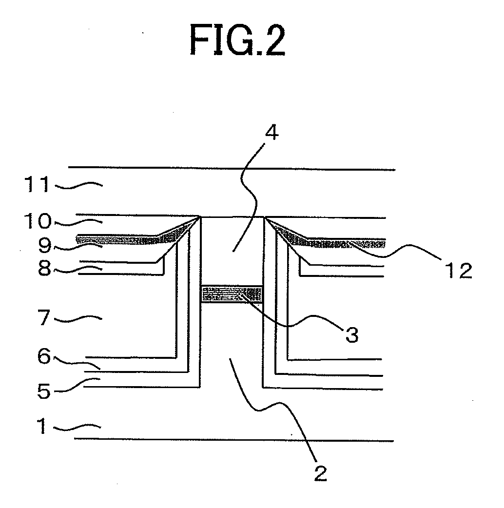
[0074]FIG. 5 is a sectional view illustrating a structure of a semiconductor optical element according to Embodiment 3 of the present invention.

[0075]In a distributed-feedback semiconductor laser illustrated in FIG. 5, three layers of the second n-type InP layer 8, the undoped i-type InP layer 9, and the second p-type InP layer 10, illustrated in FIG. 1 are replaced by an Ru-doped semiconductor layer 19.

[0076]It is to be noted that, instead of the three layers of the second n-type InP layer 8, the undoped i-type InP layer 9, and the second p-type InP layer 10, only the undoped i-type InP layer 9, two layers of the umdoped i-type InP layer 9 and the second p-type InP layer 10, or two layers of the second n-type InP layer 8 and the undoped i-type InP layer 9 may be replaced by the Ru-doped semiconductor layer 19.

[0077]Embodiment 3 has the advantage that, because almost no interdiffusion is caused between Ru and Zn, compared with the case of Embodiment 1 described above, the shapes of ...


PUM


Abstract

A semiconductor optical element and an integrated semiconductor optical element suppressing leakage current flow through a burying layer. A mesa-stripe-shaped laminate structure includes a p-type cladding layer, an active layer, and an n-type cladding layer. A burying layer on a side of the laminated structure includes, a first p-type semiconductor layer, a first n-type semiconductor layer, an Fe-doped semiconductor layer, a second n-type semiconductor layer, a low carrier concentration semiconductor layer, and a second p-type semiconductor layer. The Fe-doped semiconductor layer is not grown on a (111)B surface of the first p-type semiconductor layer and of the first n-type semiconductor layer. The second n-type semiconductor layer is not grown on a (111)B surface of the first p-type semiconductor layer, of the first n-type semiconductor layer, and of the Fe-doped semiconductor layer.

Description

BACKGROUND OF THE INVENTION[0001]1. Field of the Invention[0002]The present invention relates to a semiconductor optical element and an integrated semiconductor optical element applied to, for example, an optical communications system.[0003]2. Description of the Related Art[0004]In recent years, with regard to a semiconductor optical element, application thereof in which, from the viewpoint of power savings, temperature rise suppression of the element, and the like, high efficiency use of injected current is required, and, at the same time, operation at higher speed than ever is required is increasing. For example, when the semiconductor optical element is a buried semiconductor laser, for the purpose of materializing high efficiency, in order to inject with efficiency current into an active layer for converting electricity to light, it is necessary to suppress a reactive current flow through a buried layer which is formed on both sides of an active layer and which has a current blo...

Claims


Application Information

Patent Timeline
Patent Type & Authority Applications(United States)
IPC IPC(8): H01S5/227
CPCH01S5/2206H01S5/2275H01S5/2222
Inventor SAKAINO, GO
Owner MITSUBISHI ELECTRIC CORP
Why Eureka
Try Eureka