Method to form semiconductor laser diode
a laser diode and semiconductor technology, applied in the direction of lasers, semiconductor devices, semiconductor lasers, etc., can solve the problems of affecting the reliability of the device, serious damage to the surface of the semiconductor material, etc., to reduce the damage of the plasma, and reduce the effect of the residual carbon fluorid
- Summary
- Abstract
- Description
- Claims
- Application Information
AI Technical Summary
Benefits of technology
Problems solved by technology
Method used
Image

Examples
first embodiment
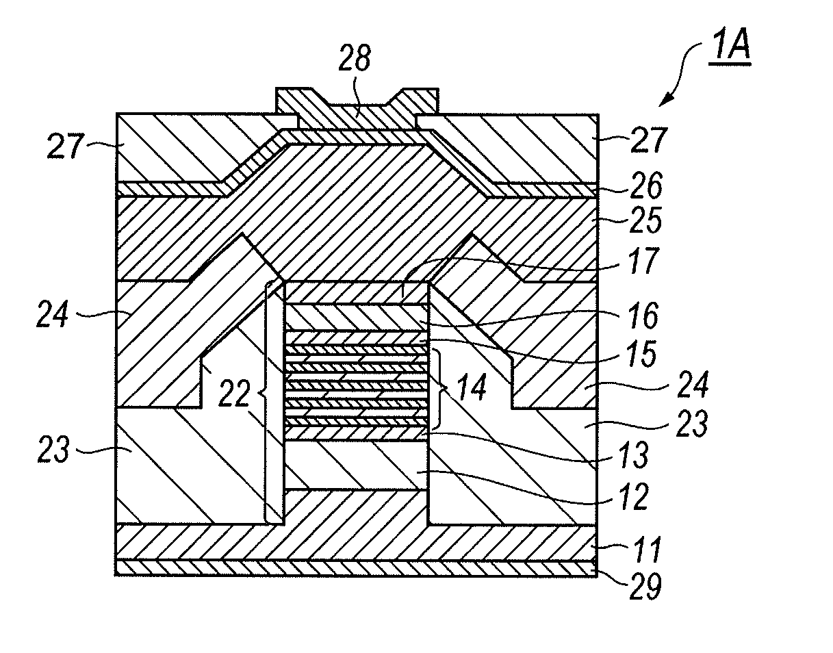
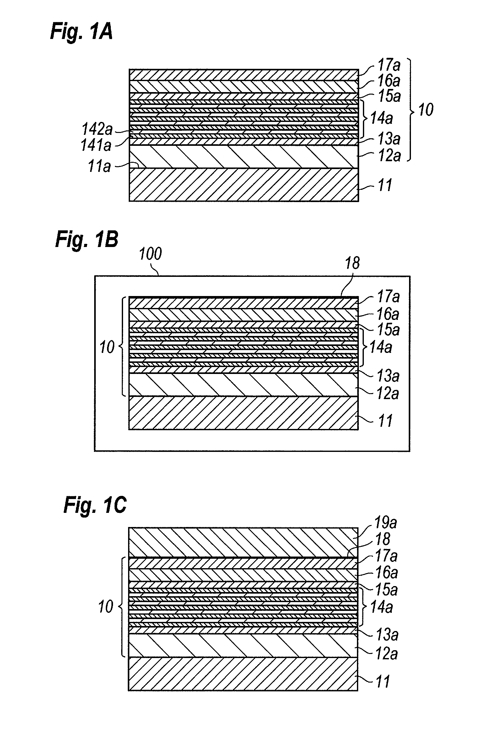
[0022]A process to manufacture a semiconductor laser diode (hereafter denoted as LD) according to an embodiment of the present invention will be described as referring to FIGS. 1 to 4. Semiconductor layers introduced in the description below may be formed by the metal organized vapor phase epitaxy (hereafter denoted as MOVPE) technique. The MOVPE uses tri-methyl-gallium (TMGa), tri-methyl-indium (TMIn), phosphine (PH3), and arsine (ArH3) for sources of gallium (Ga), indium (In), phosphorous (P), and arsenic (As), respectively. A di-ethyle-zinc (DEZn) and a mono-silane (SiH4) are used for a p-type dopant and an n-type dopant, respectively.
[0023]Formation of Layer Stack
[0024]A plurality of semiconductor layers, 12a to 17a, is grown on a primary surface 11 of an n-type InP substrate 11. These layers are provided for an active region. Specifically, the layer 12a is for the buffer layer, the layer 13a is provided for the lower optical confinement layer, the layer 14a is provided for the ...
second embodiment
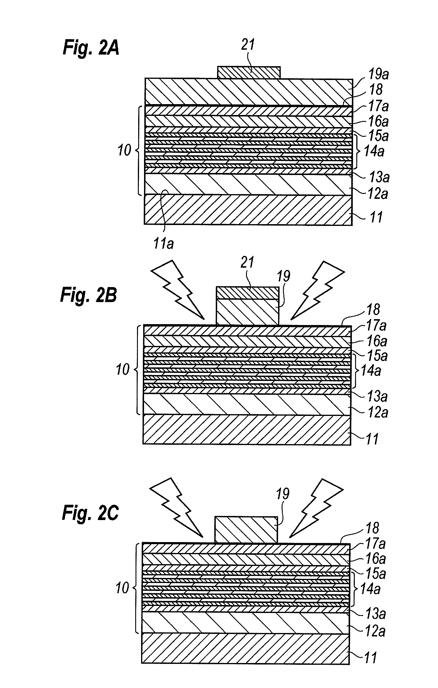
[0054]A manufacturing process according to another embodiment of the present invention will be described as referring to FIGS. 5A to 6B. Processes according to the first half until the formation of the etching mask 19, which includes the oxidization of the top of the semiconductor stack 10, are same as those of the first embodiment.
[0055]Formation of Mesa
[0056]The mesa 22 may be formed by the dry-etching using the partially etched insulating layer 19 as the etching mask, as shown in FIG. 5A. The conditions of the dry-etching are same as those shown in table 3, but the p-type cap layer made of InGaAs in the top of the mesa 22 may operate as the contact layer in the present embodiment.
[0057]Burying Mesa
[0058]As shown in FIG. 5B, the burying layer 31 is selectively grown on both sides of the mesa 22 by the insulating mask 19 as the growth mask, where the burying layer 31 may be made of iron-doped InP that shows a semi-insulating characteristic. The burying layer 31 may operate as the c...
PUM
| Property | Measurement | Unit |
|---|---|---|
| temperature | aaaaa | aaaaa |
| thickness | aaaaa | aaaaa |
| temperature | aaaaa | aaaaa |
Abstract
Description
Claims
Application Information
 - R&D Engineer
- R&D Manager
- IP Professional
- Industry Leading Data Capabilities
- Powerful AI technology
- Patent DNA Extraction
Browse by: Latest US Patents, China's latest patents, Technical Efficacy Thesaurus, Application Domain, Technology Topic.
© 2024 PatSnap. All rights reserved.Legal|Privacy policy|Modern Slavery Act Transparency Statement|Sitemap