Deposition source, thin film deposition apparatus and method of manufacturing organic light-emitting display apparatus

a technology of thin film deposition and display apparatus, which is applied in the direction of chemical vapor deposition coating, vacuum evaporation coating, coating, etc., can solve the problems of difficult formation of organic deposition layer having desired characteristics, large area, and vaporization of deposition material, so as to prevent denaturation of deposited materials and improve the characteristic of deposited thin layer easily

Inactive Publication Date: 2011-07-07
SAMSUNG DISPLAY CO LTD
View PDF30 Cites 22 Cited by
  • Summary
  • Abstract
  • Description
  • Claims
  • Application Information

AI Technical Summary

Benefits of technology

[0010]The present disclosure provides a deposition source that may prevent denaturation of deposited materials and may easily improve the characteristic of a deposited thin layer. The present disclosure also provides a thin film deposition apparatus including the deposition source, and a method of manufacturing an organic light-emitting display apparatus using the same.

Problems solved by technology

However, the deposition material may continue to be vaporized during the alignment, without operating a heater of the deposition apparatus.
Thus, the deposition material may be wasted or denatured.
However, in conventional thin film deposition apparatuses, it is difficult to form organic deposition layers having desired characteristics, on a large area.
Thus, there is a limitation in improving characteristics of the devices, using current methods.

Method used


Image

  • Deposition source, thin film deposition apparatus and method of manufacturing organic light-emitting display apparatus
  • Deposition source, thin film deposition apparatus and method of manufacturing organic light-emitting display apparatus
  • Deposition source, thin film deposition apparatus and method of manufacturing organic light-emitting display apparatus

Examples


Embodiment Construction

[0048]Reference will now be made in detail to the exemplary embodiments of the present disclosure, examples of which are illustrated in the accompanying drawings, wherein like reference numerals refer to the like elements throughout. The exemplary embodiments are described below, in order to explain the aspects of the present disclosure, by referring to the figures.

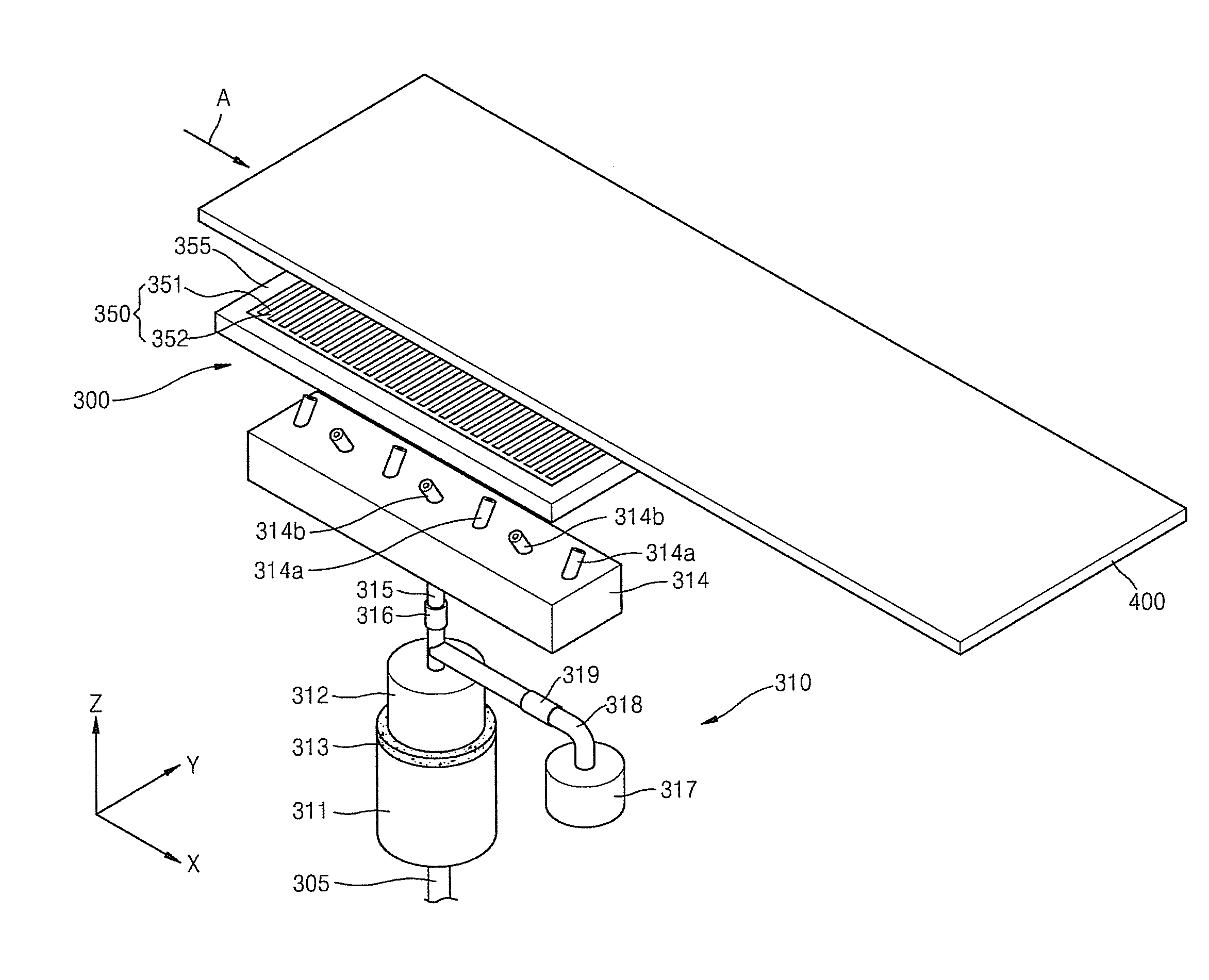
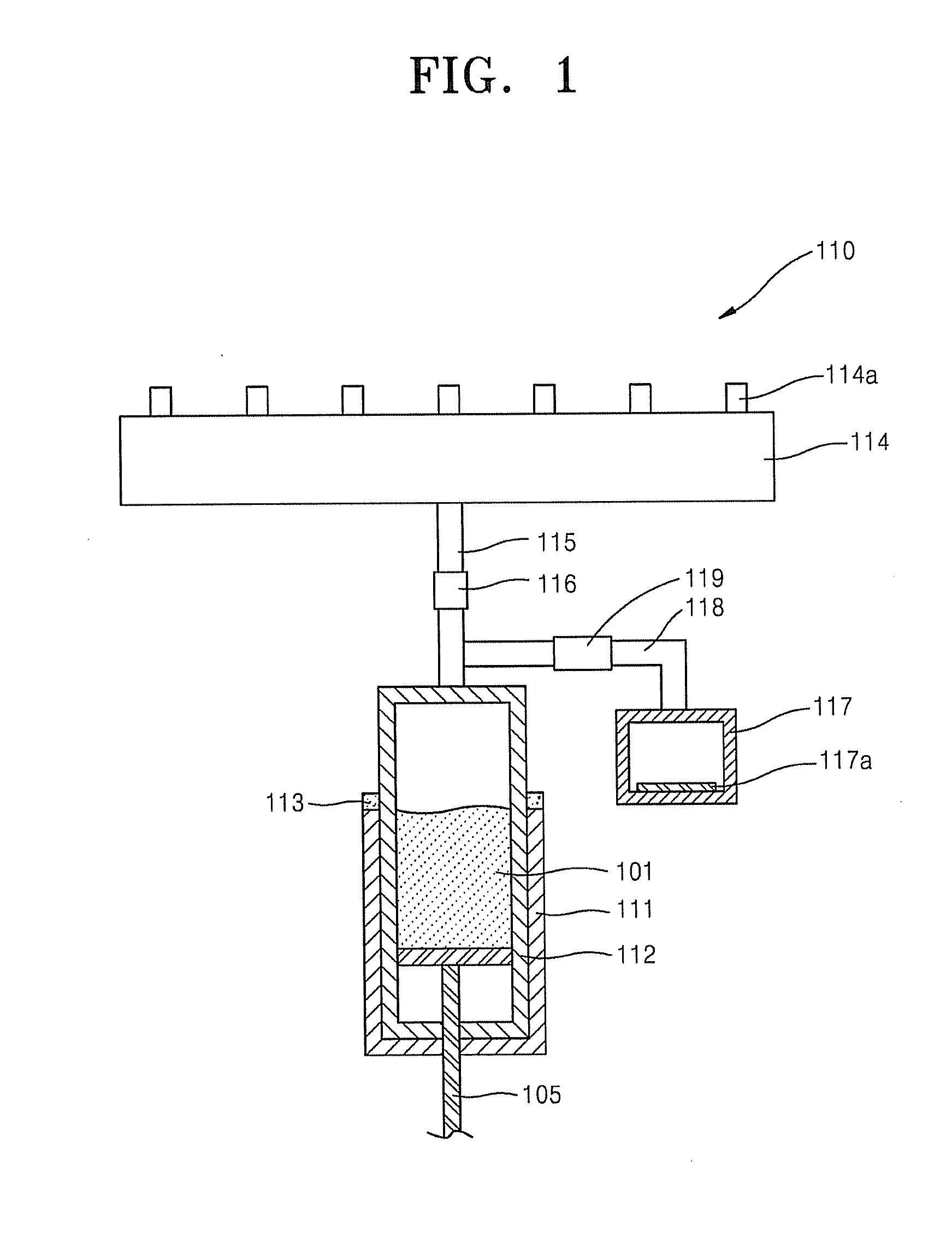
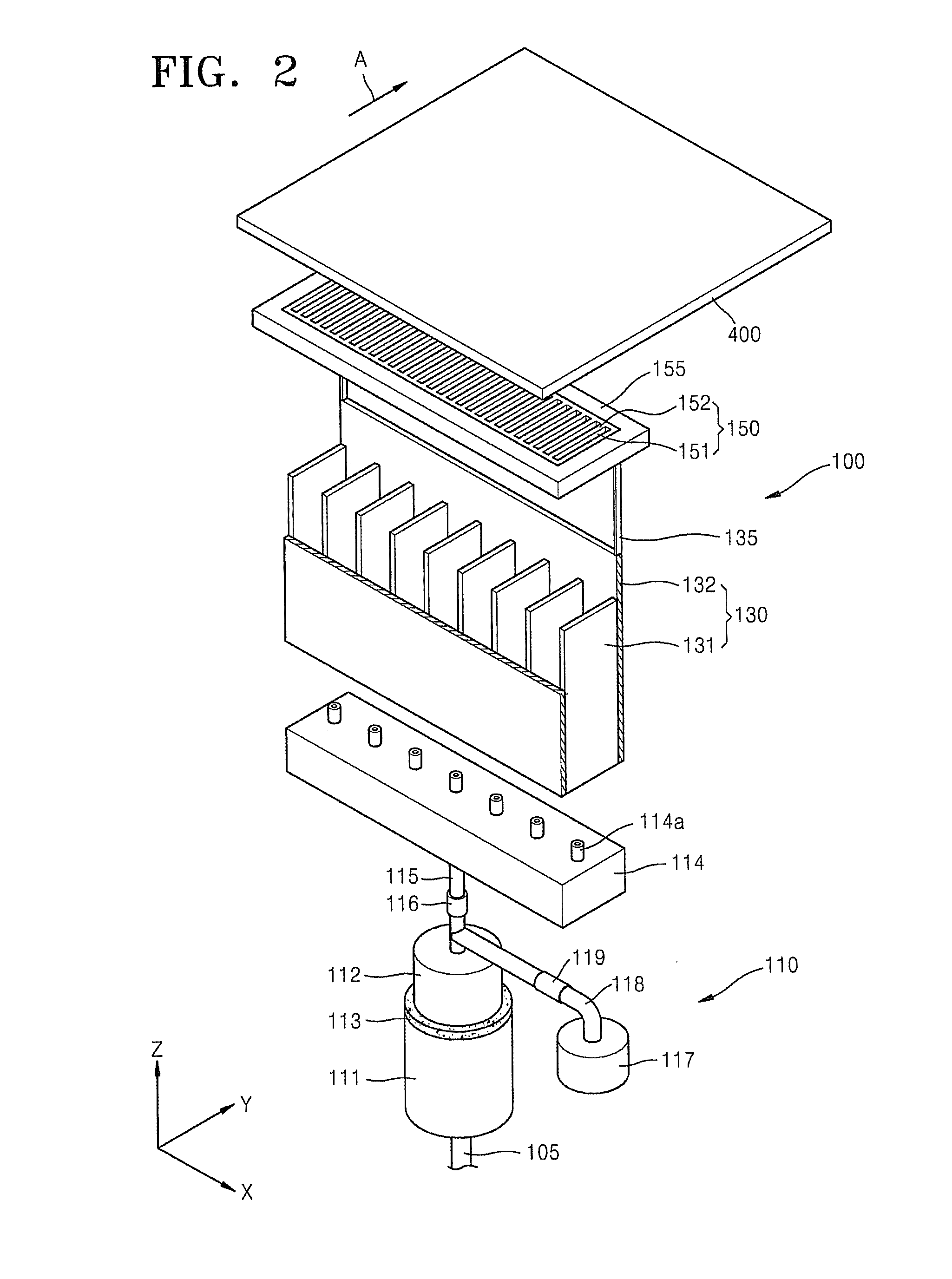
[0049]FIG. 1 is a schematic cross-sectional view of a deposition source 110, according to an exemplary embodiment of the present disclosure. Referring to FIG. 1, the deposition source 110 includes a crucible 112, a heater 113, a nozzle unit 114, a first connector 115, a first valve 116, a second connector 118, a second valve 119, and a deposition material recovery unit 117.

[0050]A deposition material 101 is filled in the crucible 112. The heater 113 is disposed around an outer circumference of the crucible 112. The heater 113 heats the crucible 112, to vaporize the deposition material 101.

[0051]The deposition source 110 m...


PUM

PropertyMeasurementUnit
temperatureaaaaaaaaaa
depositionaaaaaaaaaa
sizesaaaaaaaaaa

Abstract

A deposition source, a thin film deposition apparatus, and a method of manufacturing an organic light-emitting display apparatus, the deposition source including: a crucible to hold a deposition material; a heater to heat the deposition material; a nozzle unit disposed at a side of the crucible; a first connector disposed between the crucible and the nozzle unit; a first valve disposed on the first connector to control the flow of the deposition material to the nozzle unit; a deposition material recovery unit to collect the deposition material; a second connector to connect the first connector to the deposition material recovery unit; and a second valve to control the flow of the deposition material through the second connector.

Description

CROSS-REFERENCE TO RELATED APPLICATION[0001]This application claims the benefit of Korean Patent Application No. 10-2010-0000897, filed on Jan. 6, 2010, in the Korean Intellectual Property Office, the disclosure of which is incorporated herein by reference.BACKGROUND[0002]1. Field[0003]The present disclosure relates to a deposition source, a thin film deposition apparatus, and a method of manufacturing an organic light-emitting display apparatus, and method of using the same.[0004]2. Description of the Related Art[0005]Organic light-emitting display devices have a larger viewing angle, better contrast characteristics, and a faster response rate than other display devices. Thus, such devices have drawn attention as the next-generation of display device.[0006]Organic light-emitting display devices generally have a stacked structure, including an anode, a cathode, and an emission layer interposed between the anode and the cathode. The devices generally emit light when holes and electro...

Claims


Application Information

Patent Timeline
Patent Type & Authority Applications(United States)
IPC IPC(8): B05D5/06C23C16/00C23C16/44
CPCC23C14/12H01L51/56H01L51/0008C23C14/243H10K71/16H10K71/00
Inventor CHOI, YONG-SUPKANG, HEE-CHEOLCHOI, YOUNG-MOOKKIM, JONG-HEONRYU, JAE-KWANG
Owner SAMSUNG DISPLAY CO LTD
Why Eureka
Try Eureka