Method of packaging semiconductor device

a technology of semiconductor devices and packaging methods, applied in semiconductor devices, semiconductor/solid-state device details, electrical equipment, etc., can solve the problems of expensive procedures, inconvenient production inspection methods, and difficult visual inspection techniques to check the quality of solder joints

Inactive Publication Date: 2011-07-07
FREESCALE SEMICON INC
View PDF11 Cites 6 Cited by
  • Summary
  • Abstract
  • Description
  • Claims
  • Application Information

AI Technical Summary

Problems solved by technology

Thus, conventional visual inspection techniques to check the quality of the solder joint are difficult and time consuming to perform.
Optical and X-ray inspections may be performed but these procedures are expensive and require special equipment.
Micro-sectioning is another method of inspecting solder joints but this method is not really useful for production inspection.
However, after sawing, the bare metal of the lead frame is exposed.

Method used


Image

  • Method of packaging semiconductor device
  • Method of packaging semiconductor device
  • Method of packaging semiconductor device

Examples


Embodiment Construction

[0017]The present invention is illustrated by way of example and is not limited by the accompanying figures, in which like references indicate similar elements.

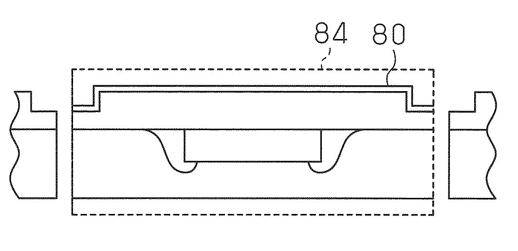
[0018]In one embodiment, the present invention provides a method of packaging a plurality of semiconductor devices. The method includes providing a lead frame strip including a plurality of individual lead frames. Each lead frame has a plurality of leads, and each lead has a first end and a second end. The leads extend outwardly from a generally rectangular central space. The first ends of the leads are proximate to the central space and the second ends are distal from the central space. One or more die pads are disposed in the central space, and saw streets are located between adjacent lead frames of the plurality of lead frames.

[0019]The method includes attaching semiconductor dies on respective first ones of the one or more die pads of the individual lead frames. Each die has an integrated circuit formed therein. Next, the...


PUM


Abstract

Quad Flat No-Lead packaged devices are manufactured using two singulation operations with two different saw blades of varying widths with the first singulation operation using a wider saw blade than the second singulation operation. Between singulation operations, the exposed portions of the leads are plated with a solderable metal. By performing the second singulation operation within the first cut made by the first singulation, at least half of the exposed metal of the leads remains plated. Thus, better solder joints may be formed, which allows for simpler visual inspection.

Description

BACKGROUND OF THE INVENTION[0001]The present invention relates generally to semiconductor device packaging, and more particularly to a method of plating and separating a lead frame of a packaged device from the lead frames of other packaged devices.[0002]There is a continuous drive to make electrical appliances such as computers, televisions, stereos, cell phones, etc. smaller, which drives the need for more highly integrated semiconductor devices in smaller packages. That is, there is a need for semiconductor devices with smaller foot prints. One type of semiconductor package is known as a Quad Flat Pack (QFP). FIG. 1 is a side cross-sectional view of a QFP device 10. The QFP device 10 includes a semiconductor die 12, which is an integrated circuit formed in Silicon, attached to a flag 14 of a lead frame with epoxy 16. The die 12 is electrically connected to leads 18 with wires 20, typically via a wire bonding process. The die 12, flag 14, wires 20 and part of the leads 18 are enca...

Claims


Application Information

Patent Timeline
Patent Type & Authority Applications(United States)
IPC IPC(8): H01L21/78H01L21/98H01L21/60
CPCH01L21/4842H01L2924/00014H01L23/49558H01L23/49582H01L24/29H01L24/48H01L24/83H01L24/85H01L24/97H01L2224/2919H01L2224/32245H01L2224/48091H01L2224/48247H01L2224/48465H01L2224/73265H01L2224/97H01L2924/01013H01L2924/01029H01L2924/0103H01L2924/01033H01L2924/01046H01L2924/01047H01L2924/01078H01L2924/01079H01L2924/01082H01L2924/14H01L2924/19041H01L23/3107H01L2224/83H01L2924/15747H01L2224/85H01L2924/014H01L2924/01006H01L2924/01005H01L2924/0665H01L2224/45099H01L2924/00H01L2924/181
Inventor LIU, PENGGAO, XUHE, QINGCHUNQI, ZHAOBINYE, DEHONG
Owner FREESCALE SEMICON INC
Why Eureka
Try Eureka