Flowable dielectric using oxide liner

a flowable dielectric and oxide liner technology, applied in the direction of electric discharge tubes, coatings, chemical vapor deposition coatings, etc., can solve the problems of dielectric material, dielectric material, and structural features of the device having decreased spatial dimensions, so as to improve adhesion, smoothness and flowability

Active Publication Date: 2011-07-07
APPLIED MATERIALS INC
View PDF101 Cites 75 Cited by
  • Summary
  • Abstract
  • Description
  • Claims
  • Application Information

AI Technical Summary

Benefits of technology

[0006]Methods of forming silicon oxide layers are described. The methods include subsequently mixing a carbon-free silicon-containing precursor with a radical-nitrogen precursor, and depositing a silicon-and-nitrogen-containing layer on a substrate. The radical-nitrogen precursor is formed in a plasma by flowing a hydrogen-and-nitrogen-containing precursor into the plasma. Prior to depositing the silicon-and-nitrogen-containing layer, a silicon oxide liner layer is formed to improve adhesion, smoothness and flowability of the silicon-and-nitrogen-containing layer. The silicon-and-nitrogen-containing layer may be converted to a silicon-and-oxygen-containing layer by curing and annealing the film. Methods also include forming a silicon oxide liner layer before applying a spin-on silicon-containing material.

Problems solved by technology

The decreasing feature sizes result in structural features on the device having decreased spatial dimensions.
The widths of gaps and trenches on the device narrow to a point where the aspect ratio of gap depth to its width becomes high enough to make it challenging to fill the gap with dielectric material.
The depositing dielectric material is prone to clog at the top before the gap completely fills, producing a void or seam in the middle of the gap.
However, once these highly flowable materials are deposited, they have to be hardened into a solid dielectric material.
Unfortunately, the departing carbon and hydroxyl species often leave behind pores in the hardened dielectic that reduce the quality of the final material.
In addition, the hardening dielectric also tends to shrink in volume, which can leave cracks and spaces at the interface of the dielectric and the surrounding substrate.

Method used


Image

  • Flowable dielectric using oxide liner
  • Flowable dielectric using oxide liner
  • Flowable dielectric using oxide liner

Examples


Embodiment Construction

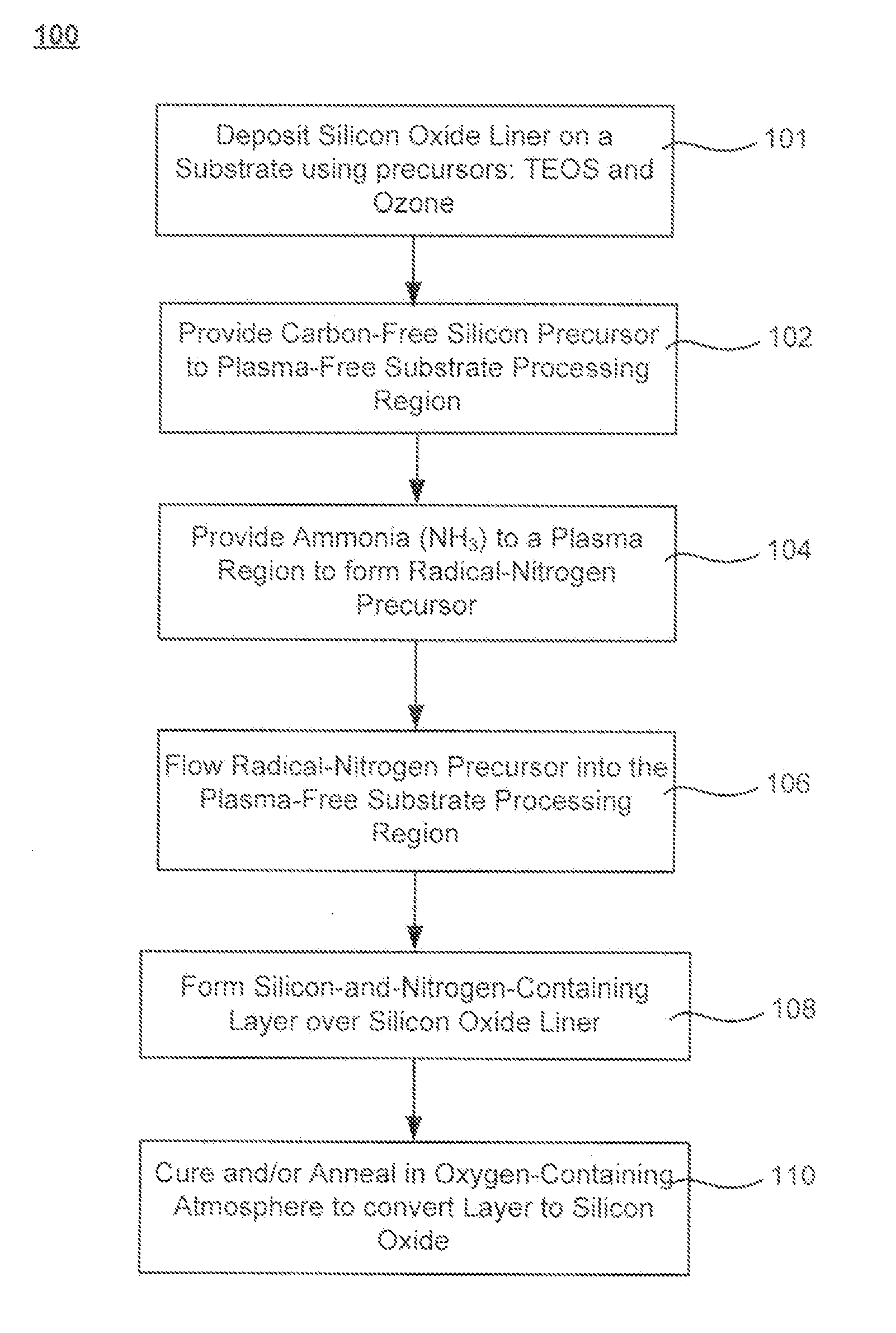
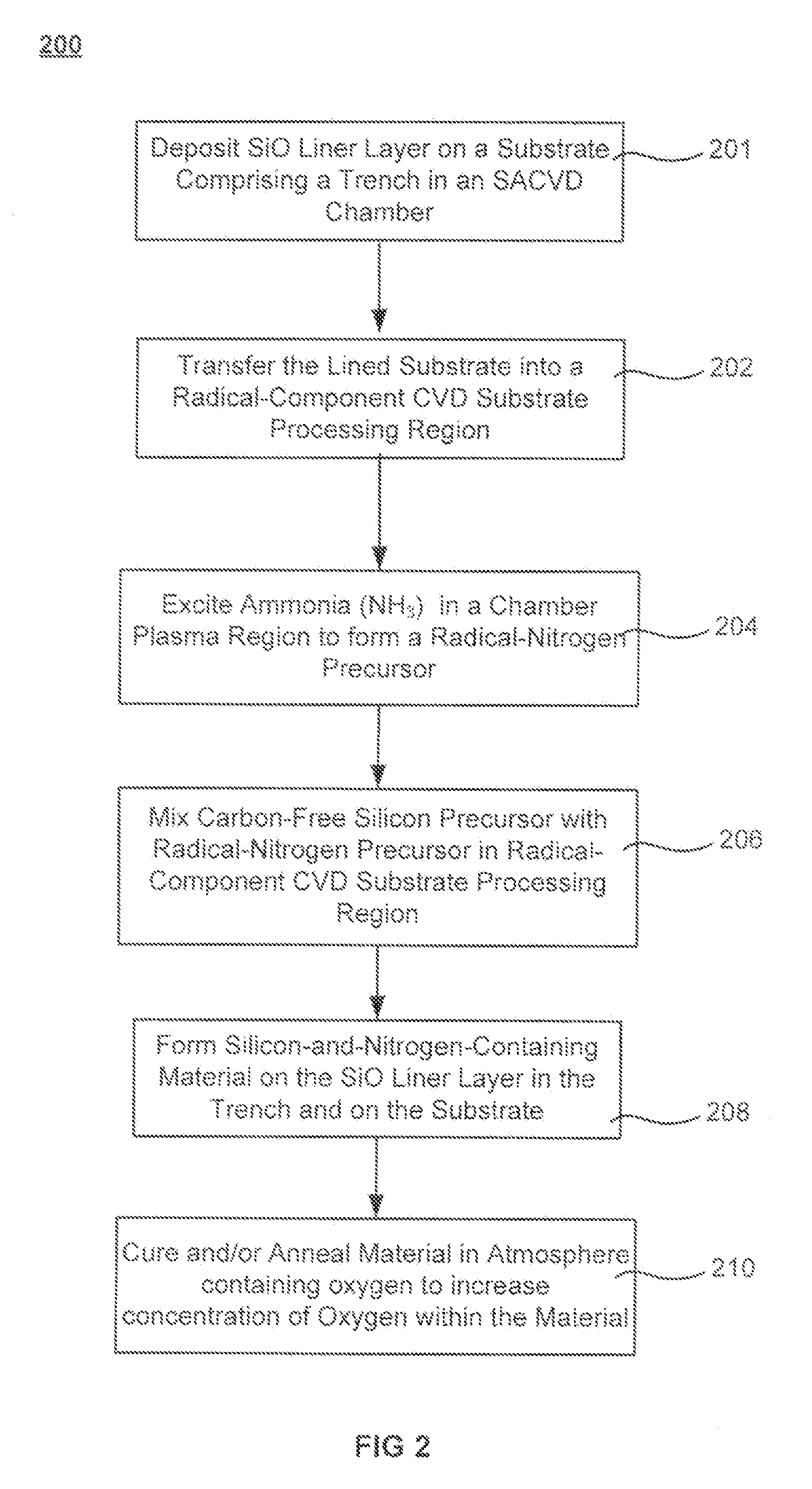
[0015]Methods of forming silicon oxide layers are described. The methods include mixing a carbon-free silicon-containing precursor with a radical-nitrogen precursor, and depositing a silicon-and-nitrogen-containing layer on a substrate. The radical-nitrogen precursor is formed in a plasma by flowing a hydrogen-and-nitrogen-containing precursor into the plasma. Prior to depositing the silicon-and-nitrogen-containing layer, a silicon oxide liner layer is formed to improve adhesion, smoothness and flowability of the silicon-and-nitrogen-containing layer. The silicon-and-nitrogen-containing layer may be converted to a silicon-and-oxygen-containing layer by curing and annealing the film. Methods also include forming a silicon oxide liner layer before applying a spin-on silicon-containing material.

[0016]Introducing an oxide liner layer between a substrate and a silicon-and-nitrogen-containing layer appears to improve adhesion and reduce incidences of delamination and cracking during and a...


PUM

PropertyMeasurementUnit
temperatureaaaaaaaaaa
deposition temperatureaaaaaaaaaa
temperatureaaaaaaaaaa

Abstract

Methods of forming silicon oxide layers are described. The methods include mixing a carbon-free silicon-containing precursor with a radical-nitrogen precursor, and depositing a silicon-and-nitrogen-containing layer on a substrate. The radical-nitrogen precursor is formed in a plasma by flowing a hydrogen-and-nitrogen-containing precursor into the plasma. Prior to depositing the silicon-and-nitrogen-containing layer, a silicon oxide liner layer is formed to improve adhesion, smoothness and flowability of the silicon-and-nitrogen-containing layer. The silicon-and-nitrogen-containing layer may be converted to a silicon-and-oxygen-containing layer by curing and annealing the film. Methods also include forming a silicon oxide liner layer before applying a spin-on silicon-containing material.

Description

CROSS-REFERENCES TO RELATED APPLICATIONS[0001]This application claims the benefit of U.S. Prov. Pat. App. No. 61 / 292,520 filed Jan. 6, 2010, and titled “RADICAL COMPONENT DIELECTRIC USING OXIDE LINER,” which is incorporated herein by reference for all purposes.BACKGROUND OF THE INVENTION[0002]Semiconductor device geometries have dramatically decreased in size since their introduction several decades ago. Modern semiconductor fabrication equipment routinely produces devices with 45 nm, 32 nm, and 28 nm feature sizes, and new equipment is being developed and implemented to make devices with even smaller geometries. The decreasing feature sizes result in structural features on the device having decreased spatial dimensions. The widths of gaps and trenches on the device narrow to a point where the aspect ratio of gap depth to its width becomes high enough to make it challenging to fill the gap with dielectric material. The depositing dielectric material is prone to clog at the top befor...

Claims


Application Information

Patent Timeline
Patent Type & Authority Applications(United States)
IPC IPC(8): H01L21/31
CPCC23C16/345C23C16/56H01J37/32357H01L21/02337H01L21/02274H01L21/02304H01L21/02326H01L21/02164H01L21/31
Inventor LIANG, JINGMEIINGLE, NITIN K.
Owner APPLIED MATERIALS INC
Why Eureka
Try Eureka