Pixel of image sensor having electrically controllable pinning layer

a technology of image sensor and pinning layer, which is applied in the direction of material analysis, radio frequency control devices, instruments, etc., can solve the problems of inability to achieve stable surface pinning, pinning layer has ground potential, and pinning layer does not have full ground potential, so as to prevent crosstalk and improve the uniformity of the reset signal between pixels

Active Publication Date: 2011-07-14
INTELLECTUAL VENTURES II
View PDF7 Cites 4 Cited by
  • Summary
  • Abstract
  • Description
  • Claims
  • Application Information

AI Technical Summary

Benefits of technology

[0026]As described above, in the image sensor according to the present invention, the pinning layer of the photodiode can be electrically controlled. In other words, the pinning layer is not in a floating state for depletion duration of the photodiode, but receives a predetermined voltage. Accordingly, stable surface pinning can beacquired.
[0027]Since uniform voltage is applied to pinning layers of photodiodes in all pixels, uniform pinning between pixels can be acquired. In addition, the uniformity of the reset signal between pixels can be improved.
[0028]Since voltage is applied to a field stop doping region, an electric field is formed from a field oxide layer to a substrate, thereby preventing crosstalk.

Problems solved by technology

However, according to the existing technology, the thickness of the depletion layer is determined only by the doping level, and the pinning layer has ground potential.
However, the pinning layer does not have full ground potential, but is put in a floating state.
As a result, the pinning layer of the photodiode in a conventional image sensor has unstable potential, so that stable surface pinning cannot be achieved.
However, in the conventional technology, uniform surface pinning between pixels cannot be acquired due to the above reasons.

Method used


Image

  • Pixel of image sensor having electrically controllable pinning layer
  • Pixel of image sensor having electrically controllable pinning layer
  • Pixel of image sensor having electrically controllable pinning layer

Examples


Embodiment Construction

[0036]Hereinafter, exemplary embodiments of the present invention will be described with reference to accompanying drawings.

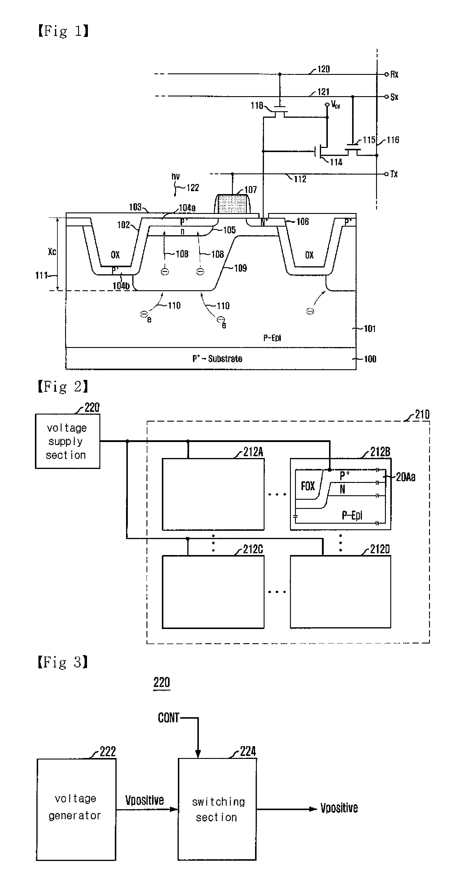
[0037]FIG. 2 is a block diagram schematically showing the structure of an image sensor according to an embodiment of the present invention.

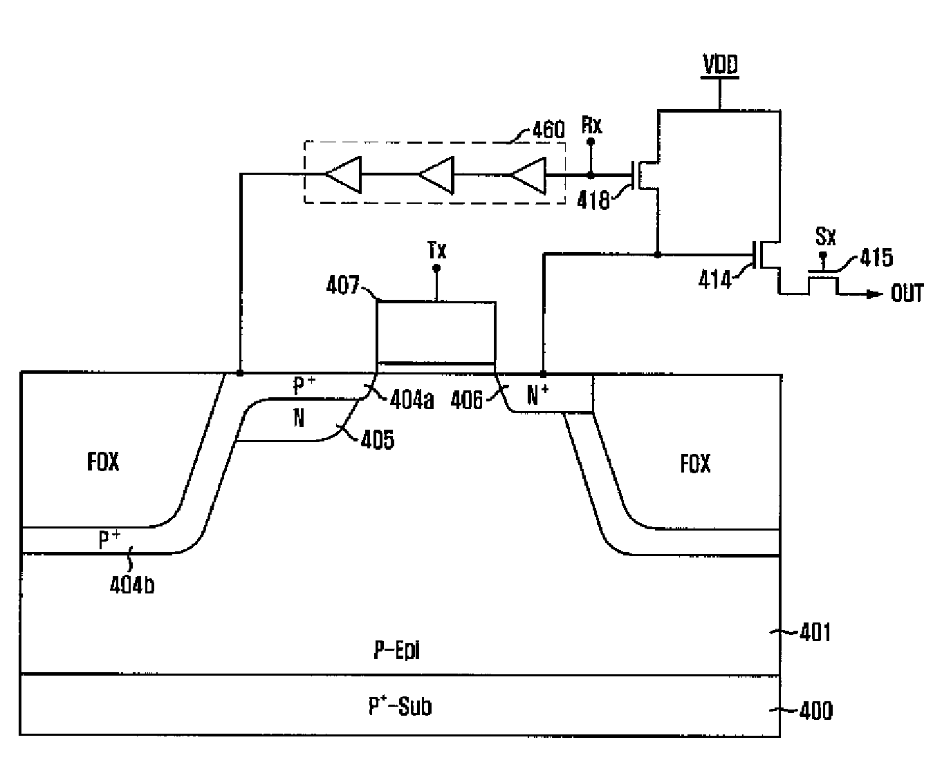
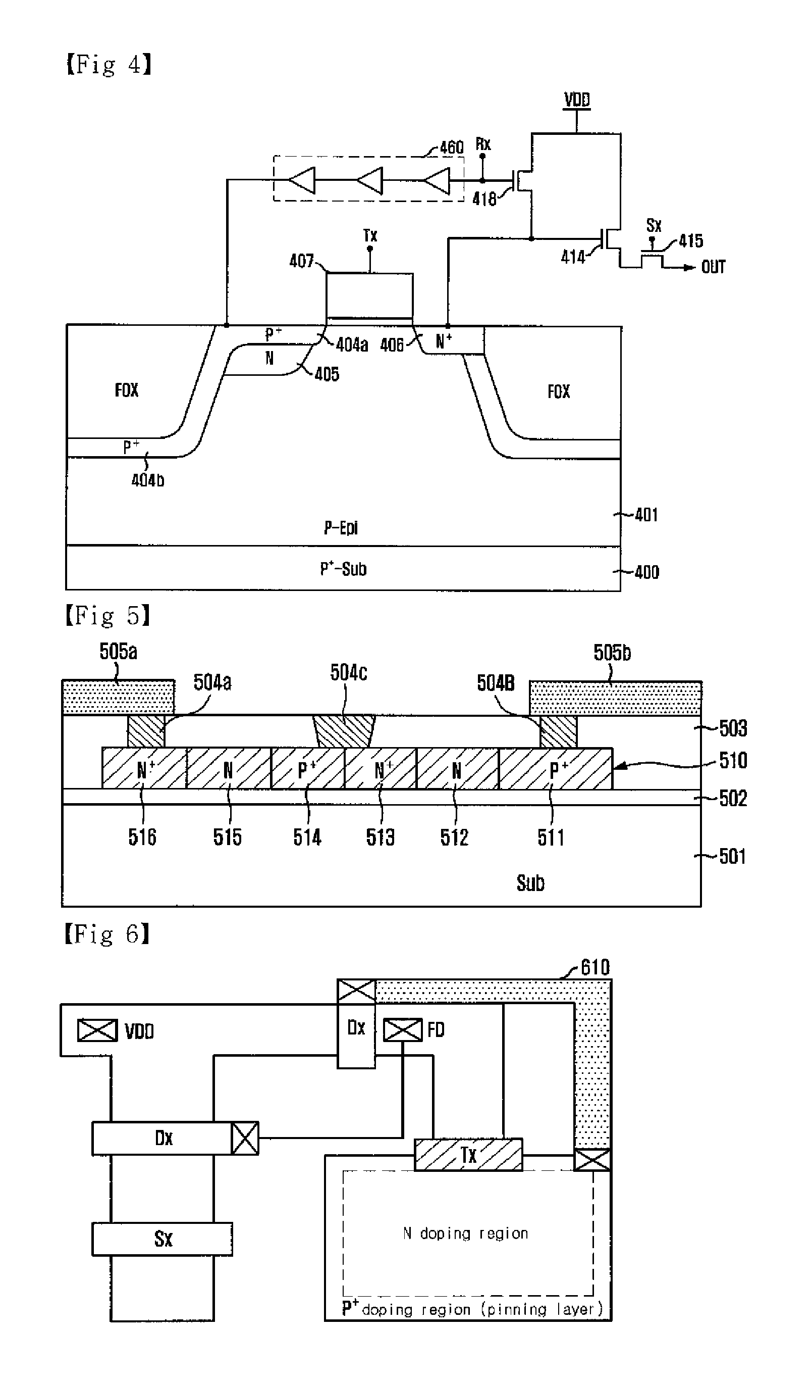
[0038]Referring to FIG. 2, pixels 212A, 212B, 212C, and 212D constituting a pixel array 210 include a pinned photodiode formed by a P+ doping region 204a and an N doping region 205 that are doping regions of a substrate P-Epi. The P+ doping region 204a serves as a pinning layer, and the pinning layer is connected to a lateral surface of a field oxide layer FOX and a field stop doping region 204b under the P+ doping region 204a.

[0039]A voltage supply section 220 generates a positive voltage of about 0.5V to about 0.9V and supplies the positive voltage to the pinning layer 204a of the pinned photodiode. The pinning layer 204a receives the positive voltage for a duration at which the pinned photodiode is depleted during the op...


PUM


Abstract

Disclosed are a pinned photodiode having and electrically controllable pinning layer and an image sensor including the pinned photodiode. A predetermined voltage is applied to the pinning layer for the depletion duration of the photodiode in the image sensor, so that stable surface pinning is acquired and the uniform surface pinning is achieved between pixels.

Description

BACKGROUND OF THE INVENTION[0001]1. Field of the Invention[0002]The present invention relates to a solid image sensor. More particularly, the present invention relates to an image sensor capable of lowering a dark current and forming a uniform depletion layer in all pixels. The present invention is applicable to all kinds of image sensors having a pinned photodiode, and is especially advantageous to a CIS (CMOS Image Sensor).[0003]2. Description of the Prior Art[0004]In general, a CMOS image sensor converts colliding photons into electrons collected in a sensor pixel to detect light. To this end, a pixel of the CMOS image sensor includes a photodiode. Especially, the pixel of the CMOS image sensor includes a pinned photodiode to reduce a dark current and increase the quantity of accumulated charges.[0005]FIG. 1 is a sectional view showing a 4 T pixel having one photodiode and 4 transistors according to the related art and illustrates a related circuit diagram.[0006]Referring to FIG....

Claims


Application Information

Patent Timeline
Patent Type & Authority Applications(United States)
IPC IPC(8): H01L27/146H01L31/113H01L31/18
CPCH01L27/14609H01L27/14689H01L27/1463H01L27/146
Inventor HA, MAN LYUN
Owner INTELLECTUAL VENTURES II
Why Eureka
Try Eureka