Organic light emitting diode display and method for manufacturing the same

Inactive Publication Date: 2011-07-14
SAMSUNG DISPLAY CO LTD
View PDF5 Cites 2 Cited by
  • Summary
  • Abstract
  • Description
  • Claims
  • Application Information

AI Technical Summary

Benefits of technology

[0028]When the gradient thickness layer becomes thinner, concentration of the metal catalyst that is scattered on the gradient thickness layer is reduced.
[0029]When the gradient of the gradient thickness layer becomes gentle, the first

Problems solved by technology

However, it is not easy to crystallize the semiconductor layer of a thin film transistor so as to simultaneously satisfy all the characteristics required for the organic light emitting diode (

Method used


Image

  • Organic light emitting diode display and method for manufacturing the same
  • Organic light emitting diode display and method for manufacturing the same
  • Organic light emitting diode display and method for manufacturing the same

Examples


Embodiment Construction

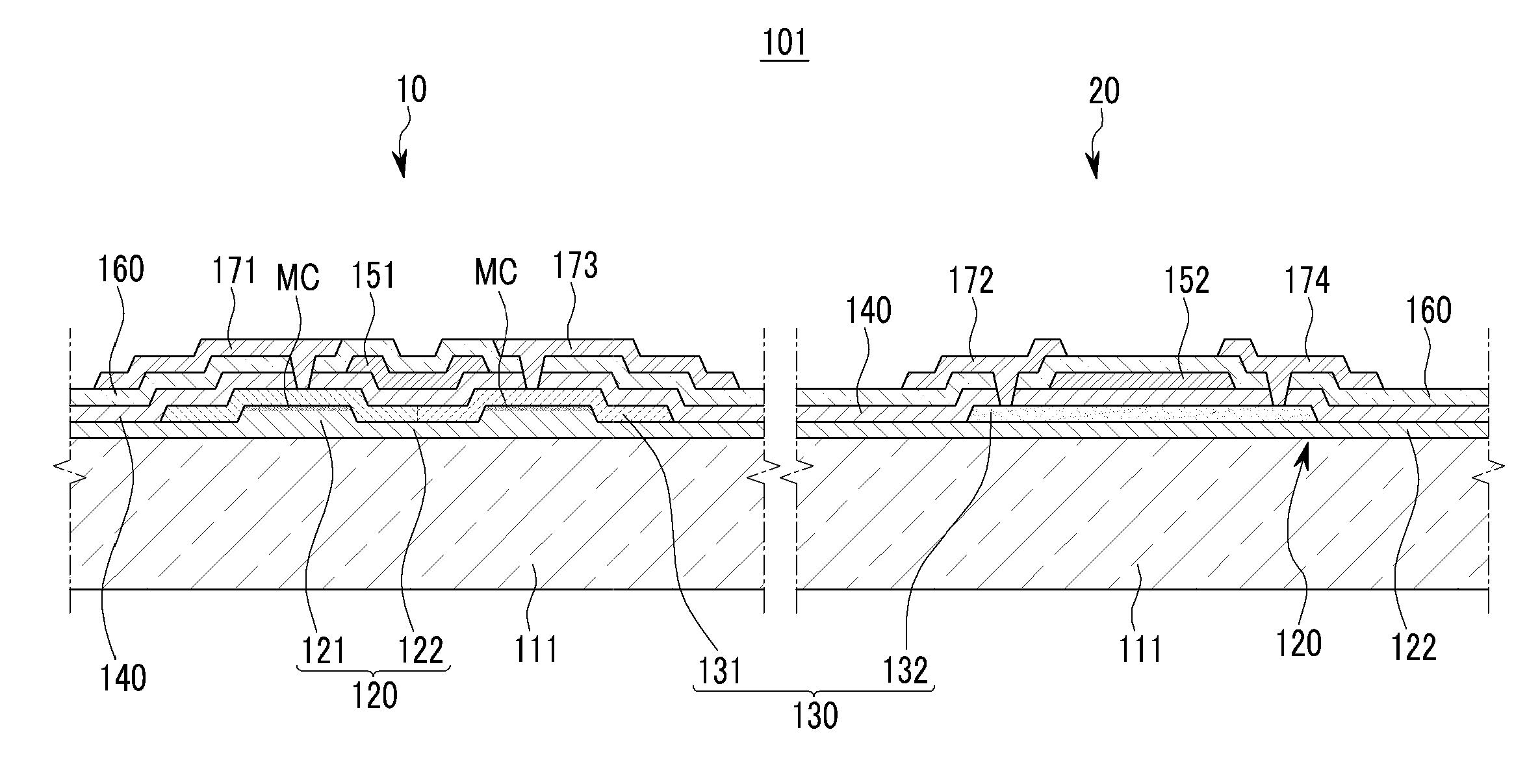
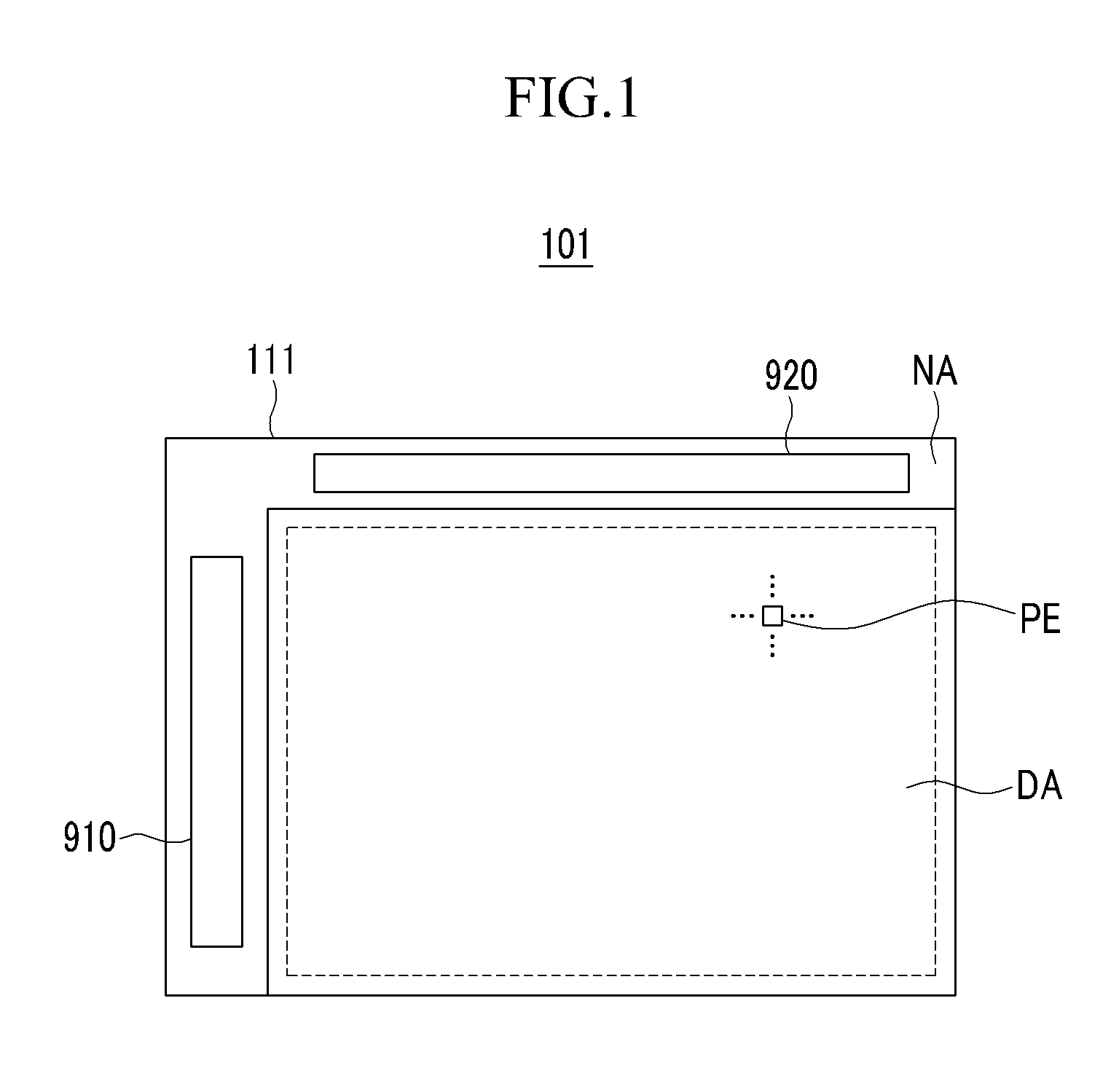
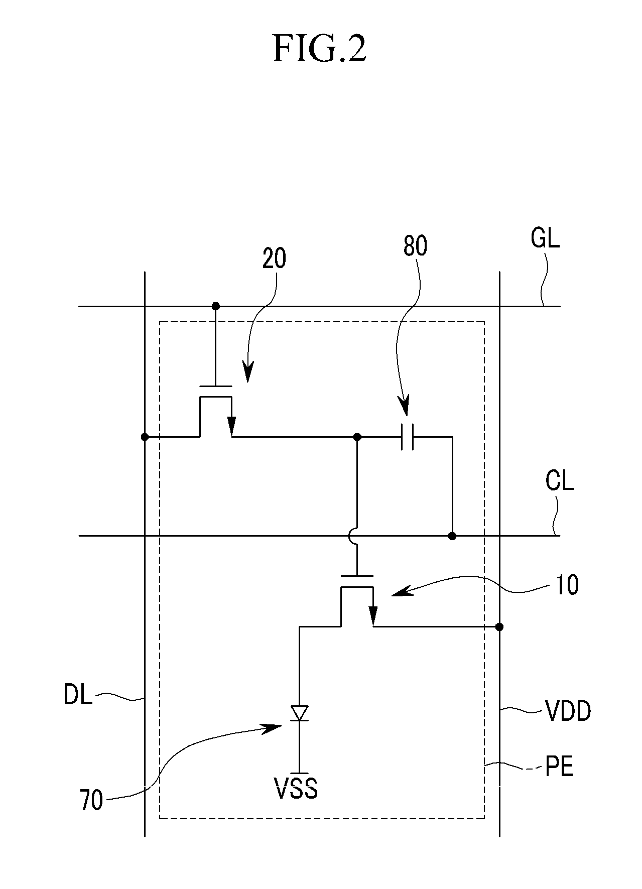
[0066]Reference will now be made in detail to the present embodiments of the present invention, examples of which are illustrated in the accompanying drawings, wherein like reference numerals refer to the like elements throughout. The embodiments are described below in order to explain the present invention by referring to the figures.

[0067]Accordingly, the drawings and description are to be regarded as illustrative in nature and not restrictive. Like reference numerals designate like elements throughout the specification. In the exemplary embodiments except the first exemplary embodiment, configurations that are different from the first exemplary embodiment will be described.

[0068]The size and thickness in the respective configurations shown in the drawings have random values for better understanding and ease of description, and they are not restricted in the exemplary embodiments.

[0069]In the drawings, the thickness of layers, films, panels, regions, etc., are exaggerated for clar...


PUM


Abstract

In an organic light emitting diode (OLED) display and a manufacturing method thereof, the OLED display includes a substrate main body; an insulation layer pattern formed on the substrate main body, and including a first thickness layer and a second thickness layer thinner than the first thickness layer; a metal catalyst that is scattered on the first thickness layer of the insulation layer pattern; and a polycrystalline semiconductor layer formed on the insulation layer pattern, and divided into a first crystal area corresponding to the first thickness layer and to a portion of the second thickness layer adjacent to the first thickness layer and a second crystal area corresponding to the remaining part of the second thickness layer. The first crystal area of the polycrystalline semiconductor layer is crystallized through the metal catalyst, and the second crystal area of the polycrystalline semiconductor layer is solid phase crystallized.

Description

CROSS-REFERENCE TO RELATED APPLICATION[0001]This application claims priority to and the benefit of Korean Patent Application No. 10-2010-0003515 filed in the Korean Intellectual Property Office on Jan. 14, 2010, the entire contents of which are incorporated herein by reference.BACKGROUND[0002]1. Field[0003]The described technology relates generally to an organic light emitting diode (OLED) display and a manufacturing method thereof. More particularly, the described technology relates generally to an organic light emitting diode (OLED) display having a polycrystalline semiconductor layer on which a plurality of thin-film transistors formed in a pixel area are crystallized by different methods according to usage, and a manufacturing method thereof.[0004]2. Description of the Related Art[0005]An organic light emitting diode display (OLED) displays images by using organic light emitting elements for emitting light. Light is generated by energy that occurs when excitons generated by a co...

Claims


Application Information

Patent Timeline
IPC IPC(8): H01L33/16
CPCH01L27/12H01L27/1251H01L27/1218H01L27/1277H01L27/1281H01L27/1285H10K59/1213H10K59/1201H05B33/10H01L21/02595H01L21/8234H01L29/66742
Inventor LEE, WON-KYUYANG, TAE-HOONCHOI, BO-KYUNGCHOO, BYOUNG-KWONMOON, SANG-HOCHO, KYU-SIKPARK, YONG-HWANCHOI, JOON-HOOSHIN, MIN-CHULLEE, YUN-GYU
Owner SAMSUNG DISPLAY CO LTD
Why Eureka
Try Eureka