Semiconductor device, manufacturing method thereof, and electronic device

a technology of semiconductor devices and manufacturing methods, applied in the direction of semiconductor devices, electrical devices, transistors, etc., can solve the problems of too many free electrons and wholly blocked active layers, and achieve the effect of stabilizing the element property of semiconductor devices, reducing manufacturing costs of semiconductor devices, and facilitating semiconductor device manufacturing

Inactive Publication Date: 2011-07-21
SHARP KK +2
View PDF14 Cites 134 Cited by
  • Summary
  • Abstract
  • Description
  • Claims
  • Application Information

AI Technical Summary

Benefits of technology

[0039]An element property of the semiconductor device can be stabilized by blocking, from the atmosphere in this way, the active layer made of the ZnO or the MgxZn1-xO each sensitive to the atmosphere. Further, the addition of the group I elements, the group III elements, the group IV elements, the group V elements, or the group VII elements to the active layer makes it possible to reduce the movable charges which are generated as the result of providing the blocking member such as the protective layer. This is explained as follows. That is, the formation of the protective layer or the like causes decrease of the surface level of the layer of, e.g., the ZnO, with the result that a depletion layer spread within the ZnO layer is eliminated. With this, the ZnO layer becomes an n-type semiconductor, with the result that too many free electrons are generated. However, for example, nitrogen of the group V elements works as an acceptor impurity with respect to the ZnO layer, so that the free electrons are reduced by adding nitrogen. Further, hydrogen of the group I elements works as a terminator with respect to the dangling bond attributing to the generation of the free electrons, while hydrogen is in ZnO. Therefore, the hydrogen addition also allows reduction of the free electrons. Such reduction of the free electrons allows decrease of the fermi level to the vicinity of the center of the band gap. This allows decrease of a gate voltage required for removal of such too many free electrons, with the result that the threshold voltage of the semiconductor device is increased. As such, the threshold voltage, which is one of important properties of a transistor, can be so controlled as to be a voltage allowing for practical use of the semiconductor device.
[0050]In this way, the ZnO or the MgxZn1-xO each sensitive to the atmosphere is blocked from the atmosphere. Moreover, the group I elements, the group III elements, the group IV elements, or the group V elements are added to the ZnO or the MgxZn1-xO. This allows reduction of the movable charges generated in the active layer by the blocking layer. This makes it possible to provide a semiconductor device whose element property is stable and is never influenced by the atmosphere, and which uses the ZnO or the MgxZn1-xO by each of which the threshold voltage can be so controlled as to fall within a voltage range allowing for the practical use of the semiconductor device.

Problems solved by technology

Further, the active layer may be wholly blocked by the blocking member.
With this, the ZnO layer becomes an n-type semiconductor, with the result that too many free electrons are generated.

Method used


Image

  • Semiconductor device, manufacturing method thereof, and electronic device
  • Semiconductor device, manufacturing method thereof, and electronic device
  • Semiconductor device, manufacturing method thereof, and electronic device

Examples


embodiment 1

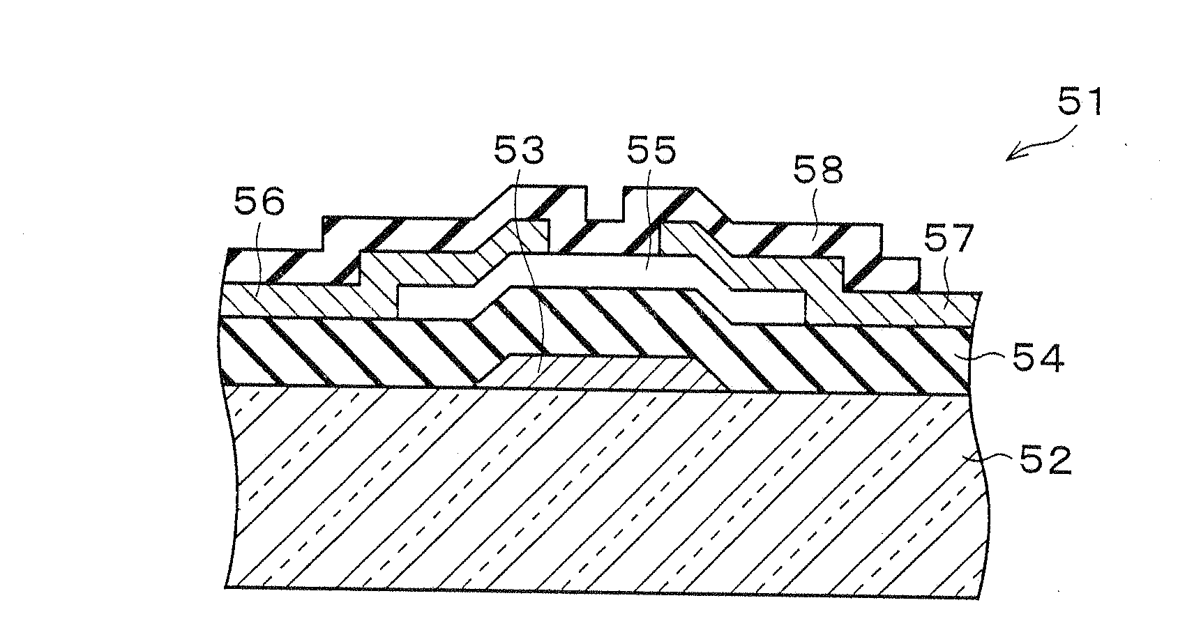
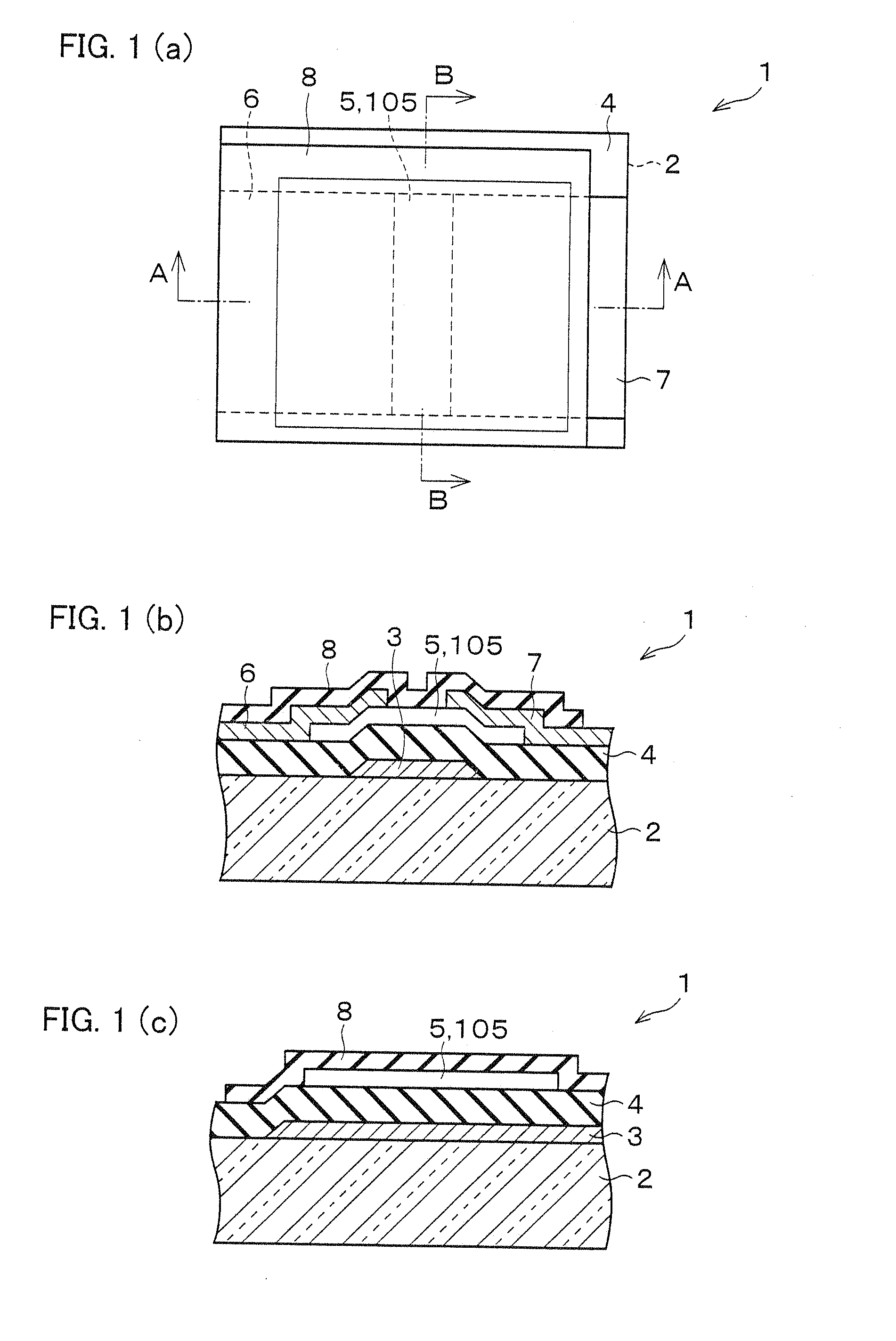
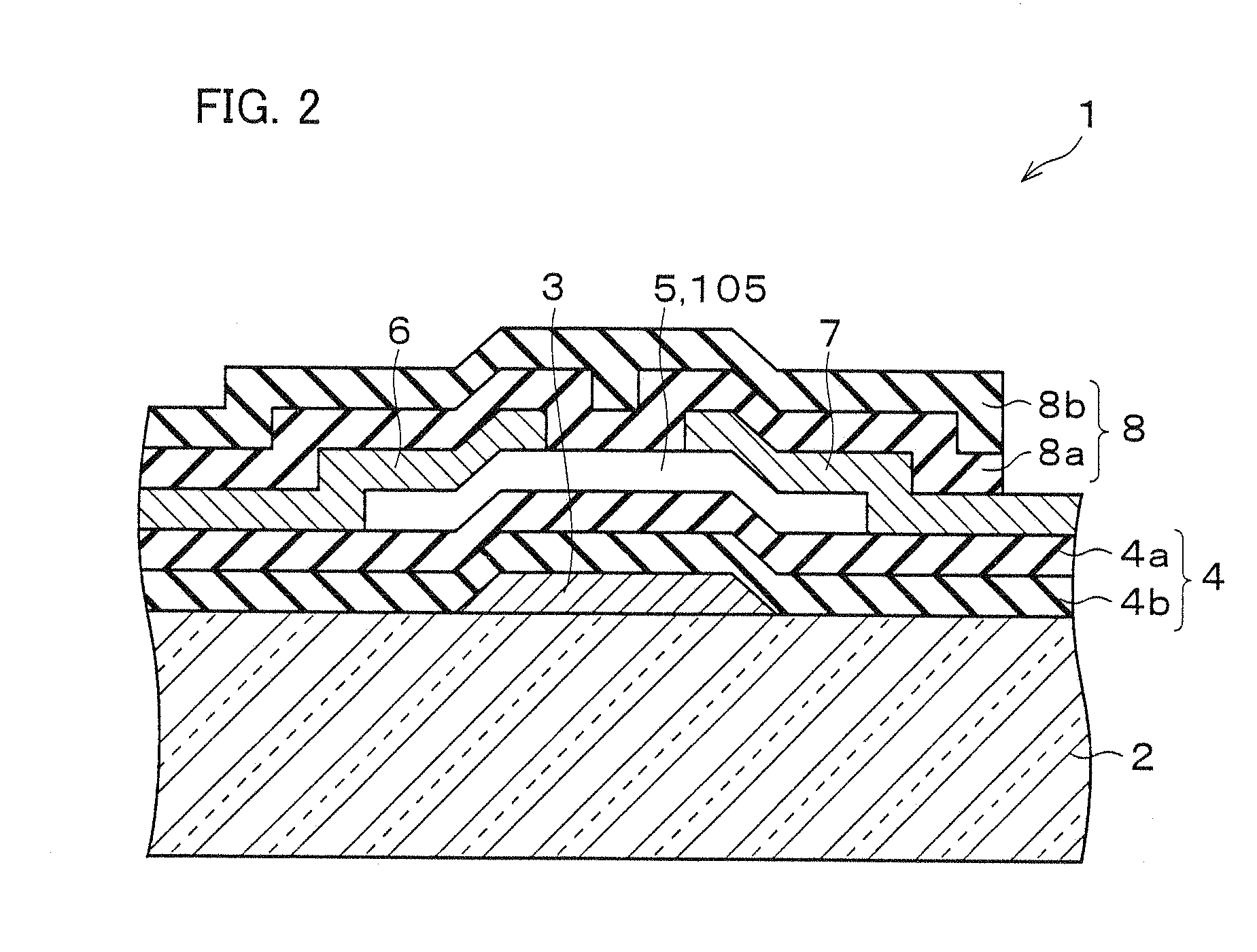
[0088]Embodiment 1 of the present invention will be explained below with reference to FIG. 1 through FIG. 5.

[0089]FIG. 1(a) is a plan view illustrating a thin film transistor 1 according to the present embodiment. FIG. 1(b) is a cross sectional view taken along line A-A of FIG. 1(a). FIG. 1(c) is a cross sectional view taken along line B-B of FIG. 1(a). Note that, although FIG. 1(b) and FIG. 1(c) describes rise and recess each formed in the central portion of the surface of a protective layer 8, FIG. 1(a) does not describe the rise and the recess for the sake of simplicity.

[0090]As shown in FIG. 1(a) through FIG. 1(c), the thin film transistor 1 serving as a semiconductor device has the inverse staggered structure. Specifically, a gate electrode 3 is formed on an insulating substrate 2. On the insulating substrate 2 and the gate electrode 3, a gate insulating layer 4 is provided. Provided on the gate insulating layer 4 is a semiconductor layer 5. Provided on the semiconductor layer ...

embodiment 2

[0110]Embodiment 2 of the present invention will be explained below with reference to FIG. 6 through FIG. 8.

[0111]FIG. 6(a) is a plan view illustrating a thin film transistor 11 according to the present embodiment. FIG. 6(b) is a cross sectional view taken along line C-C of FIG. 6(a). FIG. 6(c) is a cross sectional view taken along line D-D of FIG. 6(a). Note that, although FIG. 6(b) and FIG. 6(c) describes rise and recess each formed in the central portion of the surface of a protective layer 19, FIG. 6(a) does not describe the rise and the recess for the sake of simplicity.

[0112]As shown in FIG. 6(a) through FIG. 6(c), the thin film transistor 11 serving as a semiconductor device has the staggered structure. Specifically, a priming insulating layer 13 is formed on an insulating substrate 12. A source electrode 14 and a drain electrode 15 are formed on the priming insulating layer 13 with a space therebetween. Formed on and above the source electrode 14, the drain electrode 15, and...

embodiment 3

[0135]Embodiment 3 of the present invention will be described below with reference to FIG. 9 through FIG. 11.

[0136]FIG. 9(a) is a plan view illustrating a thin film transistor 21 according to the present embodiment. Further, FIG. 9(b) is a cross sectional view taken along line E-E of FIG. 9(a). FIG. 9(c) is a cross sectional view taken along line F-F of FIG. 9(a).

[0137]As shown in FIG. 9(a) through FIG. 9(c), the thin film transistor 21 serving as a semiconductor device is arranged as follows. That is, a priming insulating layer 23 is formed on an insulating substrate 22. Formed on the priming insulating layer 23 are a source electrode 24 and a drain electrode 25. Further, a semiconductor layer 26 is formed on the priming insulating layer 23, the source electrode 24, and the drain electrode 25. Formed on the semiconductor layer 26 is a first gate insulating layer 27. The semiconductor layer 26 and the first gate insulating layer 27 are covered with a second gate insulating layer 28 ...


PUM


Abstract

In a thin film transistor, a gate insulating layer is formed on a gate electrode formed on an insulating substrate. Formed on the gate insulating layer is a semiconductor layer. Formed on the semiconductor layer are a source electrode and a drain electrode. A protective layer covers them, so that the semiconductor layer is blocked from an atmosphere. The semiconductor layer (active layer) is made of, e.g., a semiconductor containing polycrystalline ZnO to which, e.g., a group V element is added. This allows practical use of a semiconductor device which has an active layer made of zinc oxide and which includes an protective layer for blocking the active layer from an atmosphere.

Description

CROSS-REFERENCES TO RELATED APPLICATIONS[0001]This application is a divisional of U.S. Ser. No. 10 / 560,907, filed Dec. 16, 2005, which is the U.S. national phase of international application PCT / JP2004 / 008322 filed Jun. 14, 2004, which designated the U.S. and claims priority to JP 2003-177272 filed Jun. 20, 2003, and JP 2004-079273 filed Mar. 18, 2004, the entire contents of each of which are hereby incorporated by reference.TECHNICAL FIELD[0002]The present invention relates to a semiconductor device having an active layer made of a zinc oxide. The present invention particularly relates to (i) a semiconductor device suitable for a switching element for use in an electronic device, and (ii) an electronic device using the semiconductor device.BACKGROUND ART[0003]Conventionally, zinc oxide (ZnO) is transparent in a visible light region, and is a semiconductor having a relatively good property even when prepared under a low temperature. For this reason, study on ZnO has been actively ca...

Claims


Application Information

Patent Timeline
Patent Type & Authority Applications(United States)
IPC IPC(8): H01L29/786H01L21/336
CPCH01L29/66969H01L29/7869
Inventor SUGIHARA, TOSHINORIOHNO, HIDEOKAWASAKI, MASASHI
Owner SHARP KK
Why Eureka
Try Eureka