Liquid crystal display device and manufacturing method thereof

Active Publication Date: 2011-07-21
PANASONIC LIQUID CRYSTAL DISPLAY CO LTD +1
View PDF4 Cites 23 Cited by
  • Summary
  • Abstract
  • Description
  • Claims
  • Application Information

AI Technical Summary

Benefits of technology

[0034]According to the present invention, the outer shape of the alignment film can be controlled accurately even when the alignment film i

Problems solved by technology

However, this method is disadvantageous in that when the alignment film is filled fully in the concave portion formed at the periphery of the insulating film, the alignment film further flows out to the outside.
The ITO film is formed in the concave portion at the periphery of the insulating film; however since the thickness of the ITO film is, for example, 70 nm or less, it is

Method used


Image

  • Liquid crystal display device and manufacturing method thereof
  • Liquid crystal display device and manufacturing method thereof
  • Liquid crystal display device and manufacturing method thereof

Examples


first embodiment

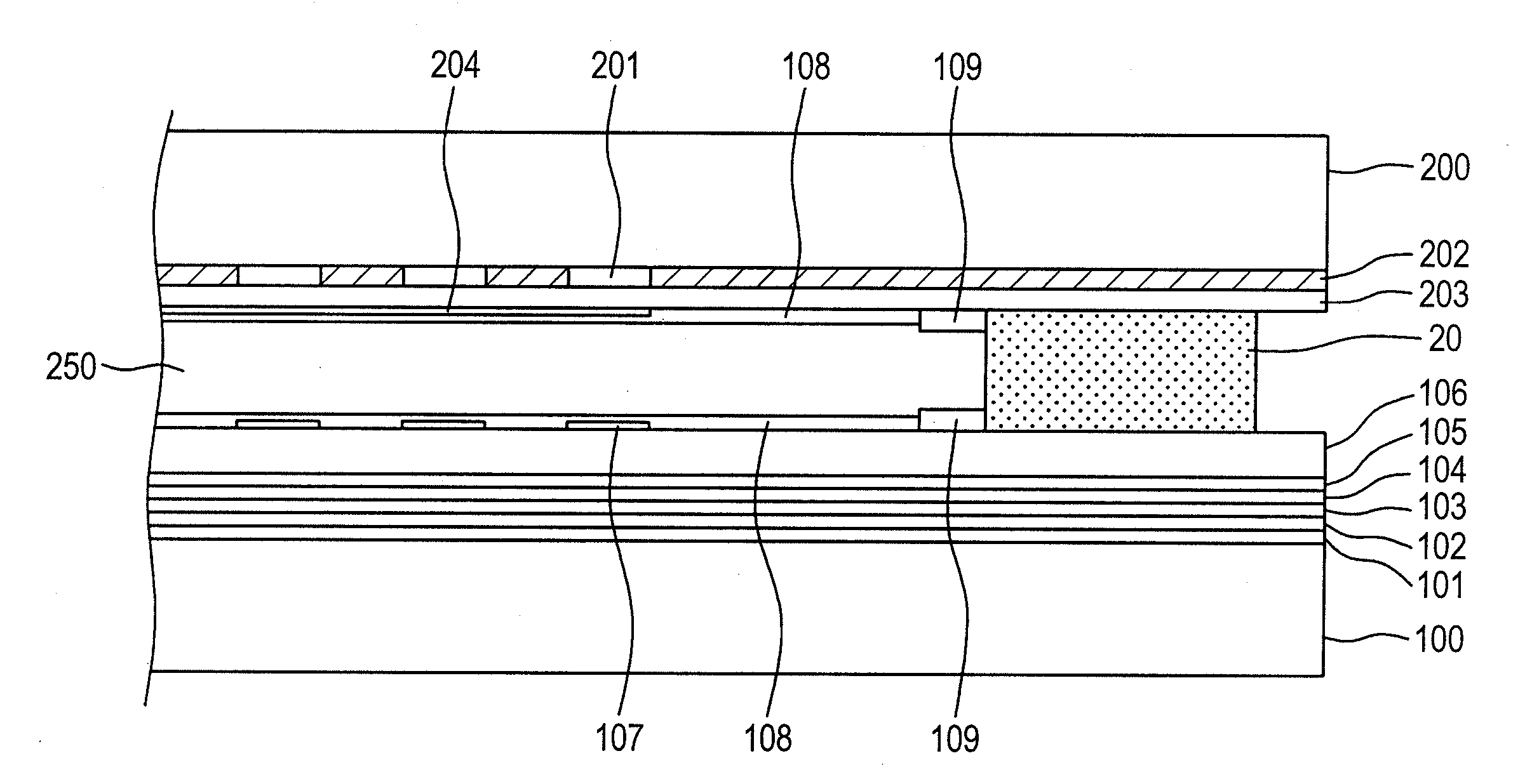
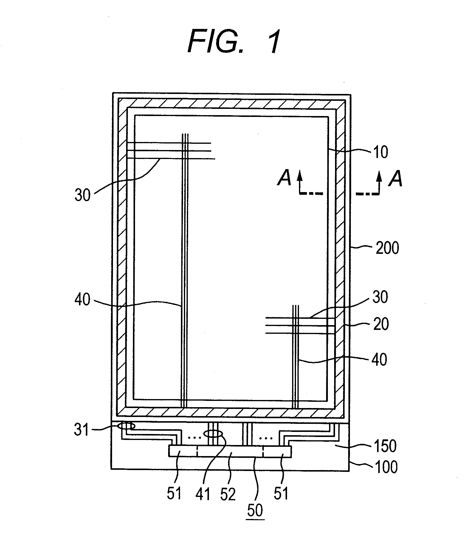
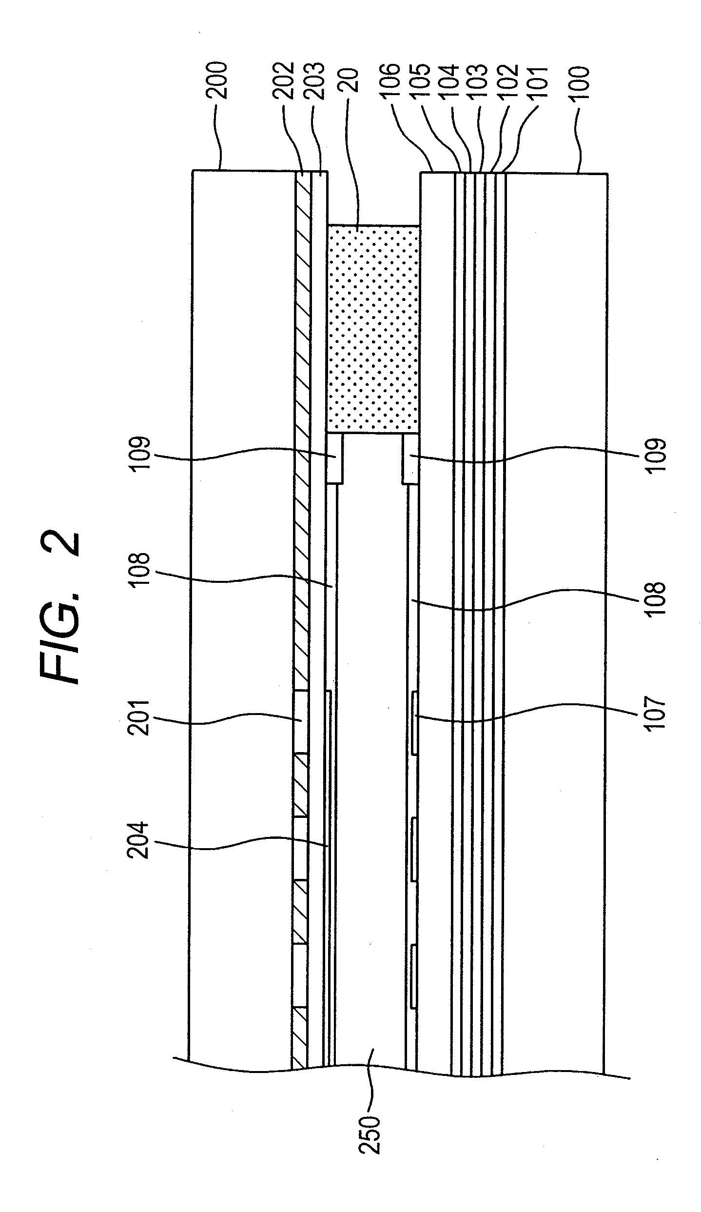
[0042]FIG. 1 is a plan view of a small-sized liquid crystal display device used for a mobile phone or the like which is an example of a product to which the invention is applied. In FIG. 1, a counter substrate 200 is disposed above a TFT substrate 100. A liquid crystal layer not illustrated is put between the TFT substrate 100 and the counter substrate 200. The TFT substrate 100 and the counter substrate 200 are bonded by a seal member 20 formed at a frame portion. In FIG. 1, since liquid crystals are sealed by one drop filling method, a sealing hole is not formed.

[0043]The TFT substrate 100 is formed larger than the counter substrate 200. A terminal portion 150 for supplying power, video signals, scanning signals, etc. to a liquid crystal display panel is formed at a portion by which the TFT substrate 100 is made larger than the counter substrate 200.

[0044]Further, an IC driver 50 for driving a scanning signal lines 30, video signal lines 40, etc. is disposed to the terminal portio...


PUM

PropertyMeasurementUnit
Thicknessaaaaaaaaaa
Sizeaaaaaaaaaa
Adhesion strengthaaaaaaaaaa

Abstract

In a liquid crystal display device small in the size and having a narrow frame, an alignment film can be coated by ink jet printing, by coating a rapidly drying peripheral alignment film 109 in the shape of a frame to a TFT substrate 100 having a display region having pixel electrode 107 and a peripheral region thereof by ink jet printing, and then coating a display region alignment film 108 drying slower but excellent in the leveling effect by ink jet printing. While the display region alignment film 108 dries slowly, since the peripheral alignment film 109 formed to the periphery functions as a stopper, the shape of the alignment film can be defined accurately, thereby enabling to prevent lowering of the adhesion of the seal member 20 under the effect of the alignment film. This can be applied also on the side of the counter substrate 200.

Description

CLAIM OF PRIORITY[0001]The present application claims priority from Japanese Patent Application JP 2010-007068 filed on Jan. 15, 2010, the content of which is hereby incorporated by reference into this application.BACKGROUND OF THE INVENTION[0002]1. Field of the Invention[0003]The present invention relates to a display device. The invention particularly relates to a liquid crystal display device that can be formed as a so-called narrow frame type in which a display region is made larger relative to a predetermined outer shape.[0004]2. Description of the Related Art[0005]A liquid crystal display device has a TFT substrate and a counter substrate opposed to the TFT substrate. The TFT substrate includes pixels arranged in a matrix, each pixel having a pixel electrode and a thin film transistor (TFT). The counter substrate includes a color filter formed at a position corresponding to a position at which the pixel electrode is located above the TFT substrate. Liquid crystals are put betw...

Claims


Application Information

Patent Timeline
IPC IPC(8): G02F1/1337B05D5/06B32B38/14
CPCG02F1/133753H01L27/1292G02F2001/133388G02F1/133388G02F1/1337G02F1/1339G02F1/133512G02F1/133514G02F1/134336G02F1/134363G02F1/13471G02F1/1368G02F2201/123
Inventor SHIROMOTO, TOMOYUKIIWATA, TOSHIROUYANG, RAISOTO, SHINICHI
Owner PANASONIC LIQUID CRYSTAL DISPLAY CO LTD
Why Eureka
Try Eureka