Video processing circuit, video processing method, liquid crystal display device, and electronic apparatus

Active Publication Date: 2011-07-28
SEIKO EPSON CORP
View PDF2 Cites 13 Cited by
  • Summary
  • Abstract
  • Description
  • Claims
  • Application Information

AI Technical Summary

Benefits of technology

[0008]An advantage of some aspects of the invention is to provide a techn

Problems solved by technology

For example, when a lateral electric field is applied to liquid crystal that should be driven by a vertical electric field as in the vertical alignment (VA) mode or the twisted nematic (TN) mode, an alignment defect of liquid crystal (reverse tilt domain) occurs, causing a display defect.
However, the technique for reducing the reverse tilt domains with the structure of the liquid crystal panel

Method used


Image

  • Video processing circuit, video processing method, liquid crystal display device, and electronic apparatus
  • Video processing circuit, video processing method, liquid crystal display device, and electronic apparatus
  • Video processing circuit, video processing method, liquid crystal display device, and electronic apparatus

Examples


Example

[0039]Hereinafter, an embodiment of the invention will be described with reference to the drawings.

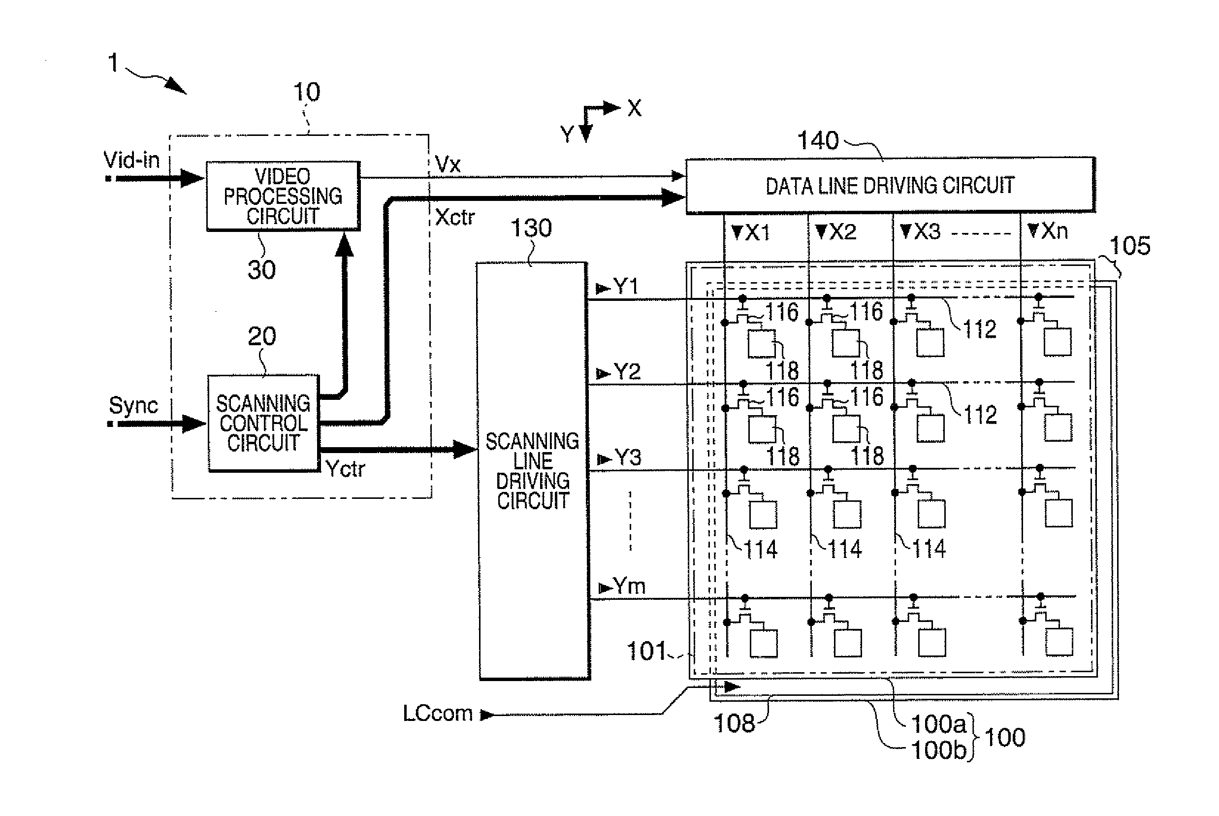
[0040]FIG. 1 is a block diagram showing the overall configuration of a liquid crystal display device to which a video processing circuit according to the embodiment is applied.

[0041]As shown in the drawing, the liquid crystal display device 1 has a control circuit 10, a liquid crystal panel 100, a scanning line driving circuit 130, and a data line driving circuit 140. To the control circuit 10, a video signal Vid-in is supplied from a higher-level device in synchronization with a synchronizing signal Sync. The video signal Vid-in is digital data that specifies a gray-scale level of each pixel in the liquid crystal panel 100 and supplied in a scanning order according to a vertical scanning signal, a horizontal scanning signal, and a dot clock signal (none of them are shown) included in the synchronizing signal Sync.

[0042]Although the video signal Vid-in specifies a gray-scale level, it ...


PUM


Abstract

A video processing circuit for a liquid crystal panel is disclosed. The video processing circuit includes: a risk boundary detecting unit configured to detect a risk boundary that is a portion of boundaries each between a first pixel whose applied voltage that is specified by an input video signal is below a first voltage and a second pixel whose applied voltage exceeds a second voltage higher than the first voltage, the risk boundary being determined by a tilt azimuth of the liquid crystal; an identification unit configured to identify a first pixel that is surrounded by the risk boundary at least two edges, in first pixels adjacent to the boundaries; and a replacement unit configured to replace, a voltage to be applied to a liquid crystal element corresponding to the first pixel, the voltage being specified by the input video signal, with a predetermined third voltage.

Description

BACKGROUND[0001]1. Technical Field[0002]The present invention relates to a technique for reducing display defects in a liquid crystal panel.[0003]2. Related Art[0004]Liquid crystal panels each include: a pair of substrates, in one of which pixel electrodes are arranged in matrix so as to correspond to respective pixels, and in the other of which a common electrode is disposed in common for the pixels; and liquid crystal interposed between the pixel electrode and the common electrode. In such a configuration, when a voltage according to a gray-scale level is applied and held between the pixel electrode and the common electrode, the alignment state of the liquid crystal is defined for each pixel, whereby the transmittance or reflectance is controlled. Accordingly, it can be said in the configuration that, among electric fields acting on liquid crystal molecules, only a component in a direction from the pixel electrode toward the common electrode (or the opposite direction), that is, a...

Claims


Application Information

Patent Timeline
IPC IPC(8): H04N3/14G09G5/00
CPCG09G3/3611G09G2310/0235G09G2340/16G09G2320/0271G09G2320/0209
Inventor HOSAKA, HIROYUKIIISAKA, HIDEHITO
Owner SEIKO EPSON CORP
Why Eureka
Try Eureka