Interface device, communications system, non-volatile storage device, communication mode switching method and integrated circuit

Active Publication Date: 2011-07-28
PANASONIC CORP
View PDF6 Cites 33 Cited by
  • Summary
  • Abstract
  • Description
  • Claims
  • Application Information

AI Technical Summary

Benefits of technology

[0064]A fourteenth aspect of the present invention provides a communication device including an external communication unit that communicates with an external unit, an external communication control unit that controls the external communication unit, and the interface device according to one of the first to twelfth aspects of the present invention.
[0065]A fifteenth aspect of the present invention provides a communications system including a host device including the interface device according to one of the thirteenth and fourteenth aspects of the present invention, and a slave device including the interface device according to one of the first to eighth aspects of the present invention.
[0066]The communications system has the same advantageous effects as the interface device of one of the first to eighth aspects of the present invention. The host device and the slave device may be included in a single apparatus, and may be connected to each other via an internal bus. In this case, the devices included in, for example, a portable terminal, have the same advantageous effects as the interface device of one of the first to eighth aspects of the present invention.
[0067]A sixteenth aspect of the present invention provides a communication mode switching method used in a communications system including at least a first transmission channel and a second transmission channel and transmitting and receiving a command and data using the two transmission channels. The method includes a mode-switching-condition detection process and a transmission-channel-switching control process.
[0068]In the mode-switching-condition detection process, a first conditio

Problems solved by technology

However, the number of terminals (pads) of an LSI, which affects the die size (chip area) and can increase the cost per chip (LSI), is limited severely.
The problem is, however, that full-duplex communication can be less efficient when, for example, communication is performed in one direction, or more specif

Method used


Image

  • Interface device, communications system, non-volatile storage device, communication mode switching method and integrated circuit
  • Interface device, communications system, non-volatile storage device, communication mode switching method and integrated circuit
  • Interface device, communications system, non-volatile storage device, communication mode switching method and integrated circuit

Examples


first embodiment

[0168]1.1 Structure of Communications System

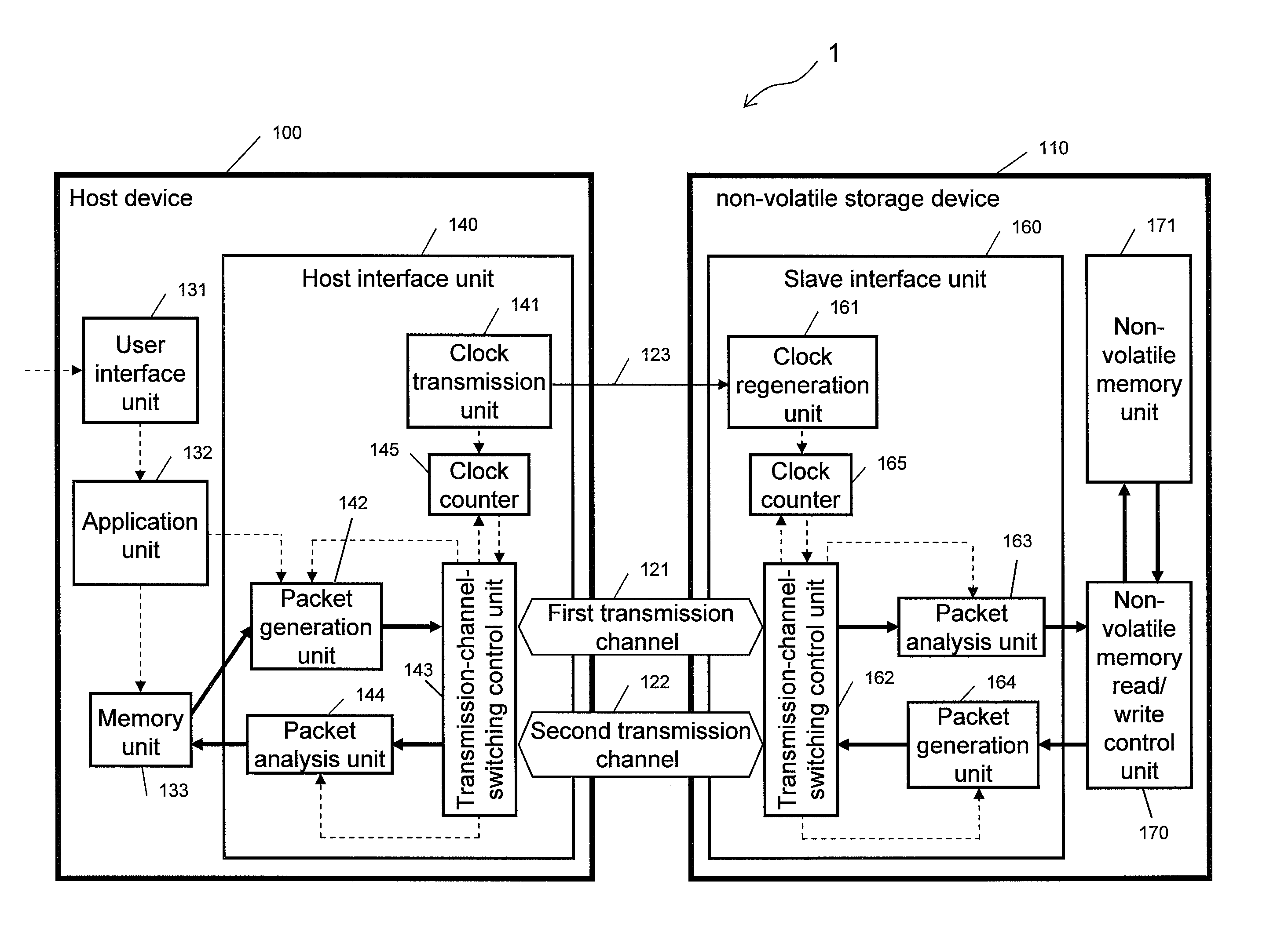
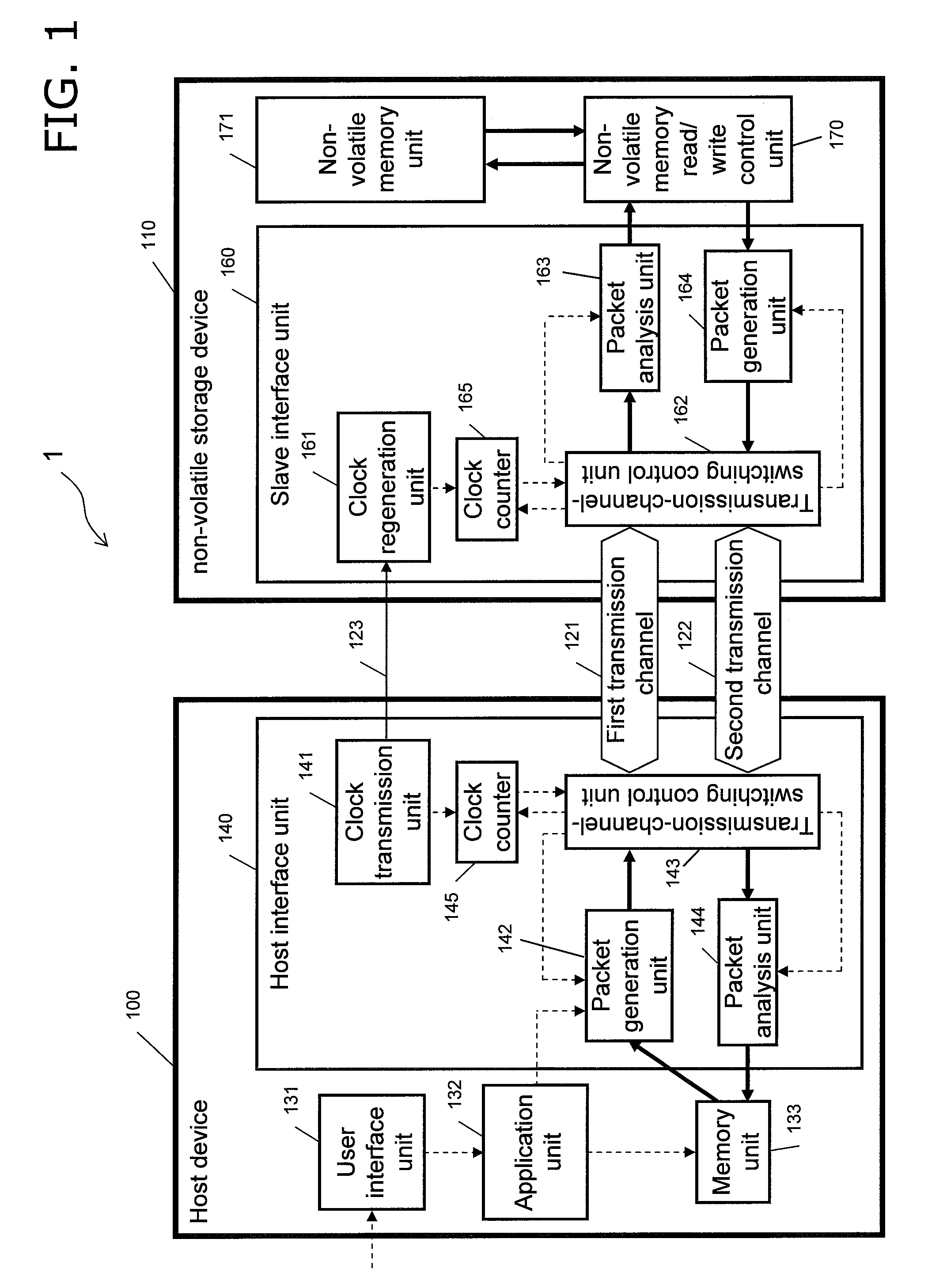
[0169]FIG. 1 is a block diagram showing the structure of a communications system 1 according to a first embodiment of the present invention.

[0170]As shown in FIG. 1, the communications system 1 includes a host device 100 and a non-volatile storage device 110, which is an example of a slave device. The host device 100 and the non-volatile storage device 110 are connected to each other with a first transmission channel 121, a second transmission channel 122, and a clock transmission channel 123.

[0171]The host device 100 includes at least a user interface unit 131, an application unit 132, a memory unit 133, and a host interface unit 140.

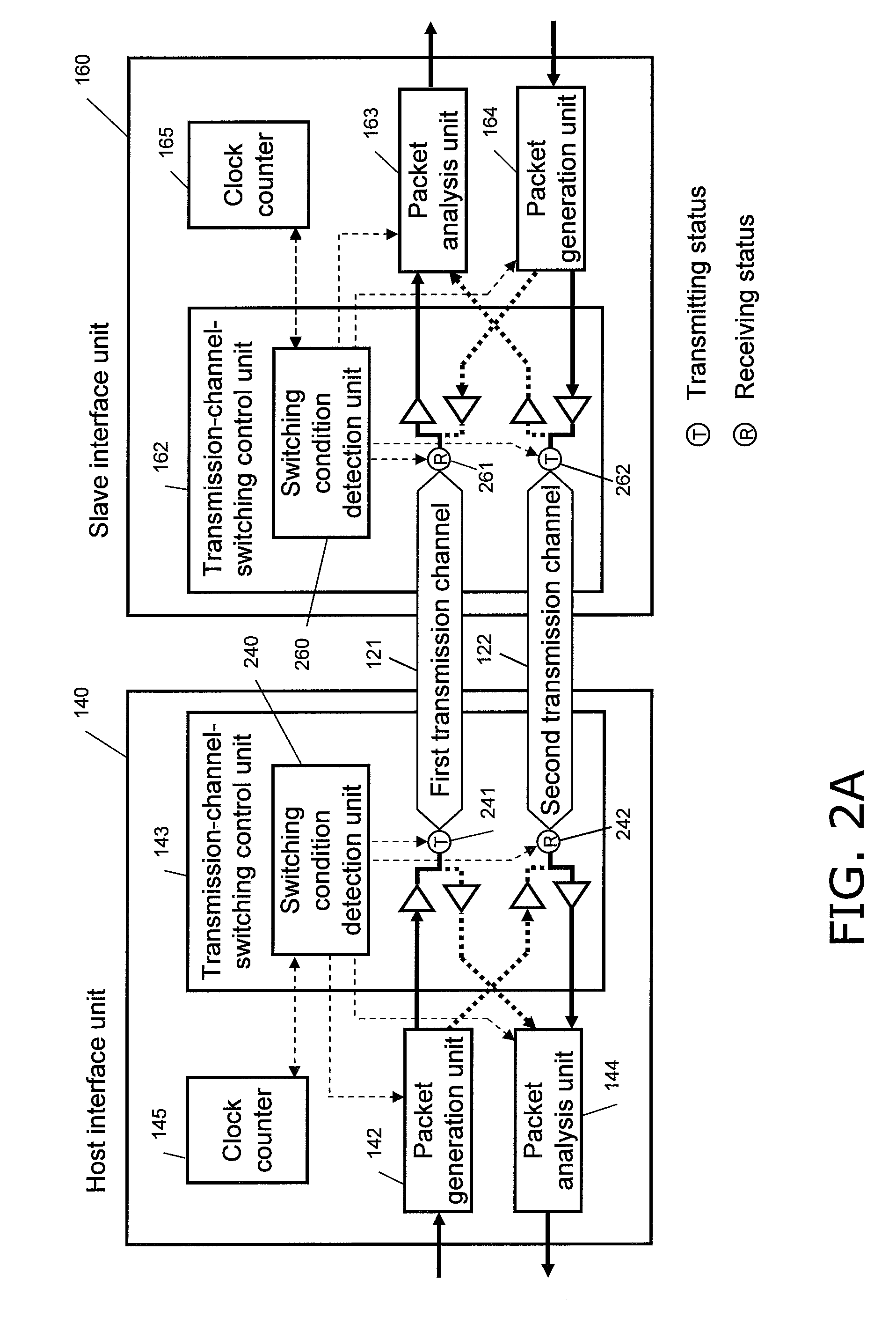
[0172]The host interface unit 140 includes a clock transmission unit 141, a packet generation unit 142, a transmission-channel-switching control unit 143, a packet analysis unit 144, and a clock counter 145.

[0173]The non-volatile storage device 110 includes at least a slave interface unit 160, a non-volatile ...

second embodiment

2.1 Structure of Communications System

[0337]FIG. 5 is a block diagram showing the structure of a communications system 2 according to a second embodiment of the present invention.

[0338]As shown in FIG. 5, the communications system 2 includes a host device 500 and a non-volatile storage device 510, which functions as a slave device. The host device 500 and the non-volatile storage device 510 are connected to each other with a first transmission channel 121, a second transmission channel 122, and a clock transmission channel 123.

[0339]The host device 500 includes at least a user interface unit 131, an application unit 132, a memory unit 133, and a host interface unit 540.

[0340]The host interface unit 540 includes a clock transmission unit 141, a packet generation unit 142, a transmission-channel-switching control unit 543, and a packet analysis unit 144. The host interface unit 540 differs from the host interface unit 140 of the first embodiment in that the host interface unit 540 doe...

third embodiment

3.1 Structure of Communications System

[0380]FIG. 8 is a block diagram showing the structure of a communications system 3 according to a third embodiment of the present invention.

[0381]As shown in FIG. 8, the communications system 3 includes a host device 800 and a non-volatile storage device 810, which functions as a slave device. The host device 800 and the non-volatile storage device 810 are connected to each other with a first transmission channel 121, a second transmission channel 122, and a clock transmission channel 123.

[0382]The host device 800 includes at least a user interface unit 131, an application unit 132, a memory unit 133, and a host interface unit 840.

[0383]The host interface unit 840 includes a clock transmission unit 141, a packet generation unit 142, a transmission-channel-switching control unit 843, and a packet analysis unit 144. The host interface unit 840 differs from the host interface unit 140 of the first embodiment in that the host interface unit 840 does...


PUM


Abstract

An interrupt request cannot be transmitted while a data read command or a data write command transmitted from a host device to a slave device is being processed in a half-duplex mode. Disclosed are a host device and a slave device that are set to a full-duplex mode by temporarily switching the communication direction of a first transmission channel or a second transmission channel after completing transmission and reception of a predetermined number of data packets in the half-duplex mode. The host device or the slave device can thus transmit an interrupt request, such as a request associated with a wait status or a busy status, to its communication target using the temporary full-duplex mode. This enables the host device or the slave device to process such an interrupt request during high-speed data transfer performed in the half-duplex mode.

Description

TECHNICAL FIELD[0001]The present invention relates to an interface device, a host device including an interface device, a slave device including an interface device, a communications system including a plurality of communication devices each of which includes an interface device, and a communication method used in the communications system.BACKGROUND ART[0002]Recent advances toward miniaturization and higher speed of semiconductors have increased the amount of data transmitted between devices or between large-scale integrated (LSI) circuits used in the devices. The communication speed of the devices or circuits is accordingly required to be higher. However, the number of terminals (pads) of an LSI, which affects the die size (chip area) and can increase the cost per chip (LSI), is limited severely.[0003]To enable high-speed data communication using less LSI terminals, many communications systems employ high-speed serial communication standards, such as USB2.0, IEEE1394, and PCI Expr...

Claims


Application Information

Patent Timeline
IPC IPC(8): H04B1/44
CPCH04L5/16H04L25/14H04L5/18
Inventor ONO, TADASHIKATO, ISAOYAMADA, HIDEYUKINISHIOKA, SHINICHIROSUENAGA, HIROSHISEKIBE, TSUTOMU
Owner PANASONIC CORP
Why Eureka
Try Eureka