Electrowetting system

a technology of electronic coding and e-mail, applied in the field of electronic coding systems, can solve the problems of large volume, large physical size of the memory store, and significant power consumption of the memory store of this speed, and achieve the effects of reducing power consumption and the required bandwidth of the display driver, efficient data transfer, and high quality

Inactive Publication Date: 2011-08-04
LIQUAVISTA BV
View PDF22 Cites 34 Cited by
  • Summary
  • Abstract
  • Description
  • Claims
  • Application Information

AI Technical Summary

Benefits of technology

[0009]Selective pixel addressing has significant advantages. Since less data needs to be sent to the display, a memory store for controlling addressing of pixels does not need to store pixel data for an entire image frame; only data relating to selected pixels for updating or refreshing needs to be stored, significantly reducing the memory size required. Further, the power consumption of the display device is significantly reduced, because significantly less information needs to be provided to update the display, compared with addressing each pixel per frame, i.e. data does not need to be sent to those elements not needing to be addressed. Also, when the information in the display state is static or is updated infrequently, the addressing rate of the display can be significantly reduced, for instance due to the fact that less information needs to be provided and that electronics may be switched off for a longer period of time at the periods where no addressing of the display occurs. Indeed, power consumption is reduced even further because no data has to be supplied to those pixels that do not change their display state, unless they are approaching the expiry of their second addressing interval. Furthermore, the data clock rate can be significantly lower, leading to a reduction of power consumption in for instance the display controller. Yet further, by addressing fewer pixels per frame, electromagnetic interference from the display is reduced and electromagnetic compatibility (EMC) is improved.
[0038]In preferred embodiments, the plurality of electrowetting elements has a first group of electrowetting elements including the first electrowetting element, and a second group of electrowetting elements including the second electrowetting element, and the display controller is arranged to address the first group twice subsequently, separated by a first addressing interval, and to address the second group twice subsequently, separated by a second addressing interval. In this way, a set of pixels, for example a block or a row of pixels, may be selectively addressed rather than individual pixels. In other words, more than one element may be addressed at the first addressing interval, and more than one element may be addressed at the second addressing interval. This may provide a more efficient scheme of updating or refreshing pixels of larger displays. Further, a memory store need only store data relating to those rows requiring addressing, meaning a smaller memory store may be used. Moreover, displays may be constructed having a faster pixel change area, and a slower pixel change / refresh area.

Problems solved by technology

However, with the miniaturisation of pixel technology and the associated increase of the number of pixels in a display, the physical size of the memory store required increases accordingly.
A memory store of this speed has a significant power consumption, which is problematic for mobile devices powered by batteries.
Moreover, such a memory store is bulky and thus occupies a large area of the substrate.
This is problematic since a substrate, for example of silicon, with the required area is expensive and would enlarge the size of the display.
A problem with this approach is that the data stored by the memory needs to be refreshed more often; for example, a memory store of 640 bits in length for the above-mentioned VGA display would need to be refreshed at a rate of 480×60 Hz.
Such a refresh rate is very high and difficult to achieve.
Further, a higher refresh rate involves greater power consumption, again causing problems for mobile applications.
Moreover, a high amount of electromagnetic interference (EMI) is produced.

Method used


Image

  • Electrowetting system
  • Electrowetting system
  • Electrowetting system

Examples


Embodiment Construction

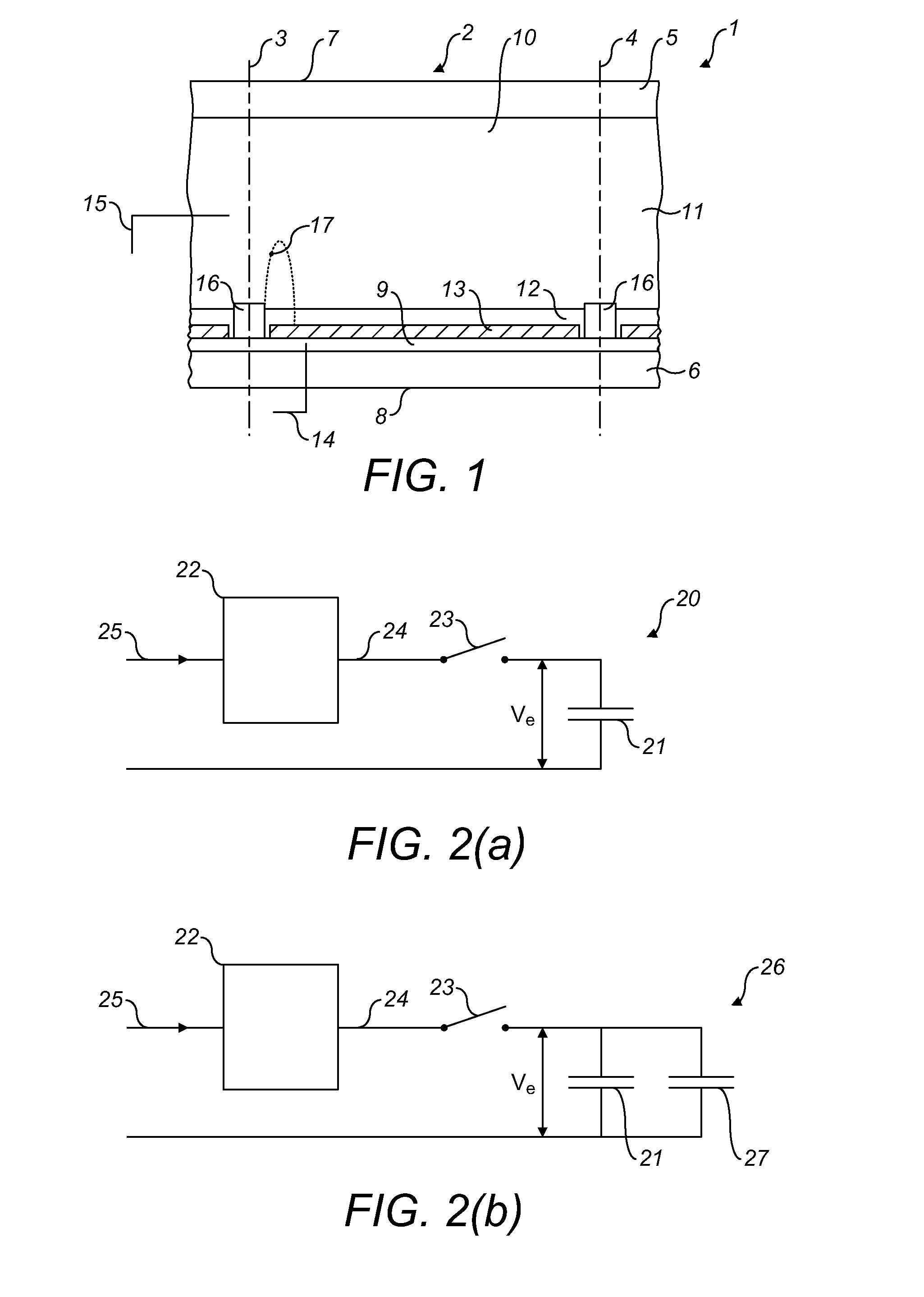
[0057]FIG. 1 shows a diagrammatic cross-section of an embodiment of an electrowetting display device 1. The display device includes a plurality of electrowetting elements 2, one of which is shown in the Figure. The lateral extent of the element is indicated in the Figure by the two dashed lines 3, 4. The electrowetting elements comprise a first support plate 5 and a second support plate 6. The support plates may be separate parts of each electrowetting element, but the support plates are preferably shared in common by the plurality of electrowetting elements. The support plates may be made for instance of glass or polymer and may be rigid or flexible.

[0058]The display device has a viewing side 7 on which an image or display formed by the display device can be viewed and a rear side 8. The first support plate 5 faces the viewing side; the second support plate 6 faces the rear side 8. In an alternative embodiment the display may be viewed from the rear side 8. The display device may b...


PUM


Abstract

An electrowetting system including a display device having a plurality of electrowetting elements, including a first electrowetting element and a second electrowetting element, each being configurable in a plurality of different display states; and a display controller for electrical addressing of the plurality of electrowetting elements in order to switch the plurality of electrowetting elements between different display states. The display controller is arranged to address the first electrowetting element twice subsequently, separated by a first addressing interval, and to address the second electrowetting element twice subsequently, separated by a second addressing interval, the second addressing interval being longer than the first addressing interval. The present invention further relates to a display controller, a driver stage and a method of controlling a display device.

Description

Cross Reference To Related Applications[0001]This Patent Application is a Continuation of International Patent Application No. PCT / EP2009 / 059967 filed on Jul. 31, 2009, entitled, “ELECTRO WETTING SYSTEM”, which claims priority to GB0814079.0 filed Aug. 1, 2008, the contents and teachings of which are hereby incorporated by reference in their entirety.FIELD OF THE INVENTION[0002]The invention relates to an electrowetting system, particularly to addressing of electrowetting elements of a display device.BACKGROUND OF THE INVENTION[0003]Pixelated displays use image data to control the display state of each pixel. Before being sent to individual pixels, this data may be stored in a memory store of a slave display module after being sent from a master display controller. The memory store maybe mounted on a substrate of the module along with the pixel matrix and associated circuitry.[0004]To refresh the image displayed, it is common for the memory store to hold data indicative of the displ...

Claims


Application Information

Patent Timeline
Patent Type & Authority Applications(United States)
IPC IPC(8): G09G5/00G02B26/00
CPCG02B26/005G09G2310/061G09G2300/0809G09G3/3433G09G3/34
Inventor SLACK, ANTHONY JOHNVAN DIJK, ROYDERCKX, HENRICUS PETRONELLA MARIA
Owner LIQUAVISTA BV
Why Eureka
Try Eureka