Duty correction circuit, delay locked loop circuit, column a/d converter, solid-state imaging device and camera system

a technology of delay locking loop circuit and duty correction circuit, which is applied in the direction of pulse technique, radio frequency controlled devices, instruments, etc., can solve the problems of unstable power consumption, reduce the number of devices, reduce the number of times of switching, and reduce power consumption

Active Publication Date: 2011-08-04
SONY CORP
View PDF7 Cites 41 Cited by
  • Summary
  • Abstract
  • Description
  • Claims
  • Application Information

AI Technical Summary

Benefits of technology

[0030]In view of the above, it is desirable to provide a duty correction circuit, a DLL circuit, a column A / D converter, a solid-state imaging device and a camera system capable of addressing both the case where the duty ratio is higher than 50% as well as the case where the duty ratio is lower than 50% by one device, therefore, it is possible not only to reduce the number of devices but also to reduce the number of times of switching, as a result, power consumption can be reduced.
[0036]According to the embodiments of the invention, both the case where the duty ratio is higher than 50% as well as the case where the duty ratio is lower than 50% can be addressed by one device, therefore, it is possible not only to reduce the number of devices but also to reduce the number of times of switching, as a result, power consumption can be reduced.

Problems solved by technology

Accordingly, not only the number of transistors is increased to some degree but the number of times of switching differs when the duty ratio of the complementary clock to be inputted is higher than 50% and when the duty ratio of the clock is lower than 50%, as a result, power consumption is not stable.

Method used


Image

  • Duty correction circuit, delay locked loop circuit, column a/d converter, solid-state imaging device and camera system
  • Duty correction circuit, delay locked loop circuit, column a/d converter, solid-state imaging device and camera system
  • Duty correction circuit, delay locked loop circuit, column a/d converter, solid-state imaging device and camera system

Examples


first embodiment

1. First Embodiment

[A First Configuration Example of a Duty Correction Circuit]

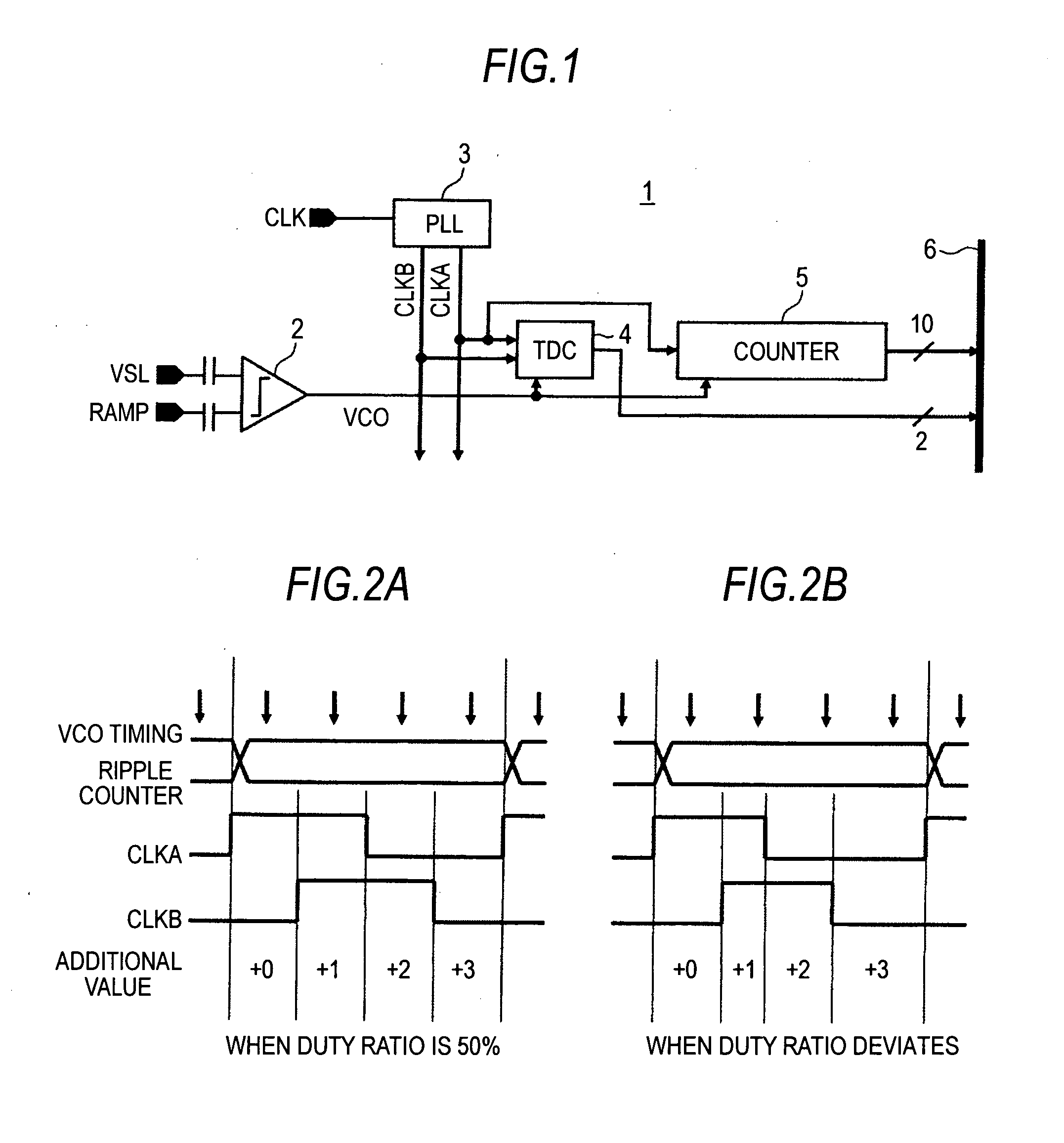
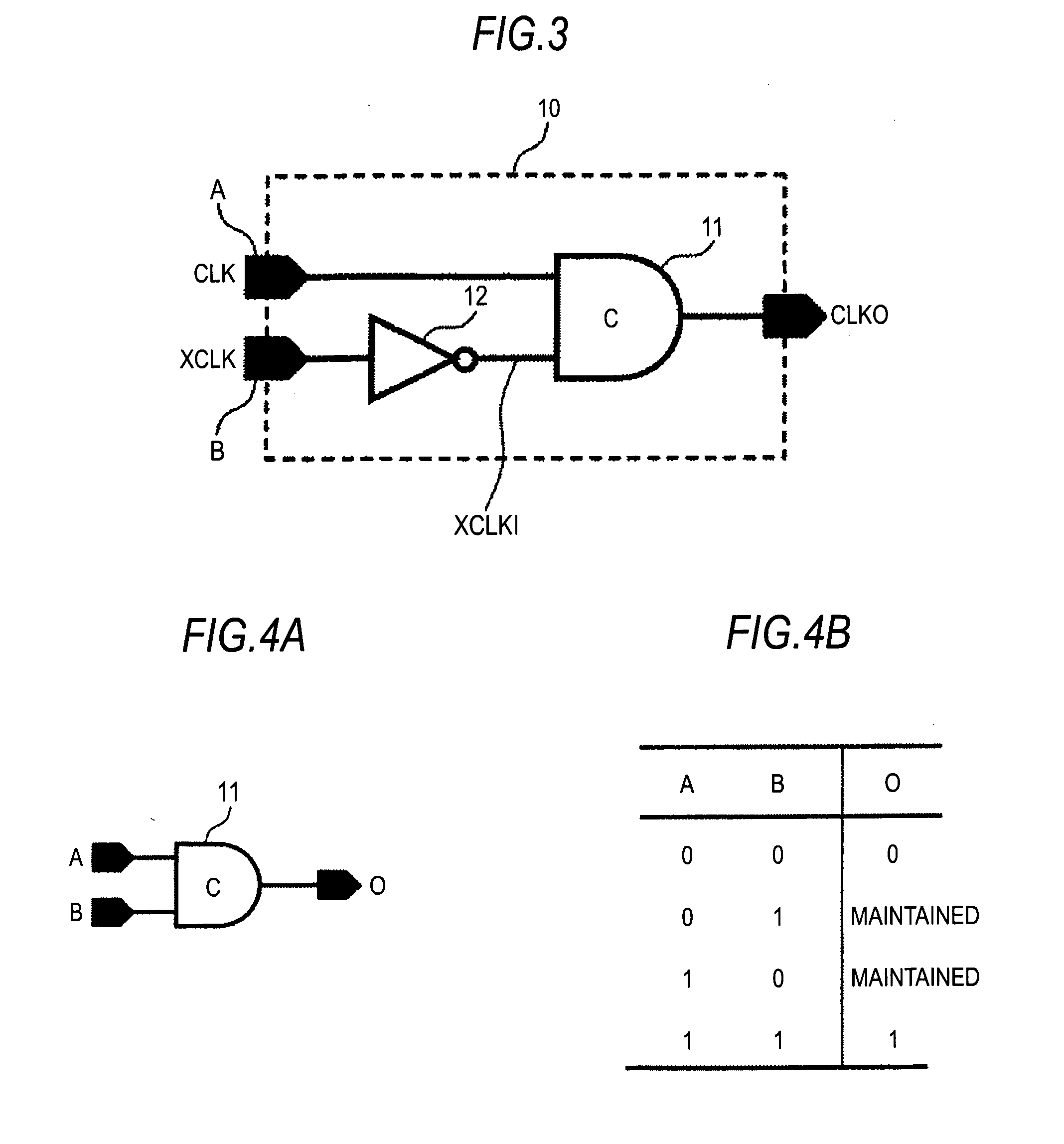
[0070]FIG. 3 is a diagram showing a configuration example of a duty correction circuit according to a first embodiment of the invention.

[0071]A duty correction circuit 10 includes one C element 11 and an inverter 12 connected to one input of the C element 11.

[0072]When complementary clocks CLK, XCLK having a phase difference of an approximately half cycle are inputted to two inputs A, B, the duty correction circuit 10 recovers the duty ratio of an output CLKO to approximately 50% even when the duty ratio of the clock signal CLK deviates.

[0073]As the C-element 11 is symmetric as explained as follows, the correction function of the duty ratio is maintained when the inverter 12 is connected to whichever input, however, the phase of the output clock is reversed.

[Function of the C-Element]

[0074]Here, a configuration and a function of the C-element will be explained.

[0075]FIGS. 4A and 4B are views showing symbo...

second embodiment

2. Second Embodiment

[Second Configuration Example of the Duty Correction Circuit]

[0151]FIG. 8 is a diagram showing a configuration example of a duty correction circuit according to a second embodiment of the invention.

[0152]A duty correction circuit 10A according to the second embodiment of the invention differs from the duty correction circuit 10 according to the first embodiment in a point that a pass-gate capacitor 13 is connected to a first input of the C-element 11 to which the inverter 12 is not connected.

[0153]Though the duty correction circuit 10 of the first embodiment can correct the duty ratio to approximately 50% in principle, delay of the inverter 12 may cause an error.

[0154]The pass-gate capacitor 13 is designed to have approximately the same delay as the inverter 12 in order to remove the error amount included in the correction circuit itself, which gives the circuit more accurate duty correction effect.

[Application Examples of the Duty Correction Circuit]

[0155]Herein...

third embodiment

3. Third Embodiment

[First Example of the Duty Correction Circuit Applied to a DLL Circuit]

[0156]FIG. 9 is a diagram showing a configuration example of a DLL circuit according to a third embodiment of the invention.

[0157]The above duty correction circuit 10 is applied to a DLL circuit (Delay Locked Loop) circuit 20. That is, the DLL circuit 20 is configured as a DLL circuit with the duty correction function.

[0158]The DLL circuit is a circuit for controlling delay time of an external interface generated due to wiring load and so on to adjust synchronization with an internal clock.

[0159]The DLL circuit 20 includes a phase detector (PD) 21, a charge pump (CP) 22, a low-pass filter (LPF) 23 and delay elements 24-1 to 24-6 connecting in cascade to an input terminal T21 of the clock CLK.

[0160]The DLL circuit 20 includes duty correction circuits 10-1, 10-2.

[0161]The DLL circuit is different from the PLL circuit, which has a characteristic in which the input clock CLK with a deviated duty ra...


PUM


Abstract

A duty correction circuit includes: a C-element including a first input and a second input; and an inverter connected to the second input of the C-element, wherein the C-element obtains an output of a logic “1” when both inputs are the logic “1”, obtains an output of a logic “0” when both inputs are the logic “0”, and maintains the output to a previous state in other conditions, and complementary clocks having a phase difference of an approximately half cycle are inputted to the first input of the C-element and the inverter respectively.

Description

BACKGROUND OF THE INVENTION[0001]1. Field of the Invention[0002]The present invention relates to a duty correction circuit correcting a clock duty ratio, a delay locked loop circuit (DLL circuit), a column A / D converter, a solid-state imaging device and a camera system using the duty correction circuit.[0003]2. Description of the Related Art[0004]Generally, in a logic circuit including a sequential circuit and a combination circuit, the sequential circuit is latch-operated to be synchronized with a clock signal.[0005]A flip flop which is a storage device used for the sequential circuit has minimum values in which the device can be operated in a width of a Hi-period and a width of a Low-period of a clock input waveform respectively.[0006]When the clock duty ratio is shifted from 50%, limitations to high-speed operation may be previously determined in the flip flop in view of the clock width.[0007]The minimum values are determined with respect to the width of the Hi-period and the wid...

Claims


Application Information

Patent Timeline
Patent Type & Authority Applications(United States)
IPC IPC(8): H04N5/335H03K3/017H03L7/06H03M1/56H01L27/146H03K5/13H03K5/19H03L7/08H03L7/081H04N5/341H04N5/369H04N5/374H04N5/376H04N5/378
CPCH01L27/146H03K3/017H04N5/335H03M1/56H03L7/06H04N25/00H03K5/1565
Inventor TAKAHASHI, TOMOHIRO
Owner SONY CORP
Why Eureka
Try Eureka