Jitter suppression circuit and jitter suppression method

a jitter suppression circuit and circuit technology, applied in the direction of pulse manipulation, pulse automatic control, pulse technique, etc., can solve the problems of jitter suppression characteristics degraded, change of parameters, and difficulty in satisfying both shortening of pull-in time and high jitter suppression characteristics, so as to shorten the pull-in time and achieve high jitter suppression

Active Publication Date: 2011-08-11
NEC CORP
View PDF8 Cites 4 Cited by
  • Summary
  • Abstract
  • Description
  • Claims
  • Application Information

AI Technical Summary

Benefits of technology

[0024]According to the present invention, in a jitter suppression circuit using a digital phase locked loop, both of shortening of a pull-in time and a high jitter suppression effect can be satisfied by determining whether the loop is in a synchronous state or not using a phase difference between the input clock and the output clock, and then changing characteristics of a loop filter according to the determination result.

Problems solved by technology

So, when the above-mentioned method is applied just as it is, as a result of mis-determination that it is in the asynchronous state when it is, in reality, in a synchronous state, an unnecessary change of a parameter occurs, and the jitter suppression characteristics degrades.
Therefore, there is a problem that it is difficult to satisfy both of shortening of a pull-in time and high jitter suppression characteristics.

Method used


Image

  • Jitter suppression circuit and jitter suppression method
  • Jitter suppression circuit and jitter suppression method
  • Jitter suppression circuit and jitter suppression method

Examples


example 1

[0038](Structure of the Example)

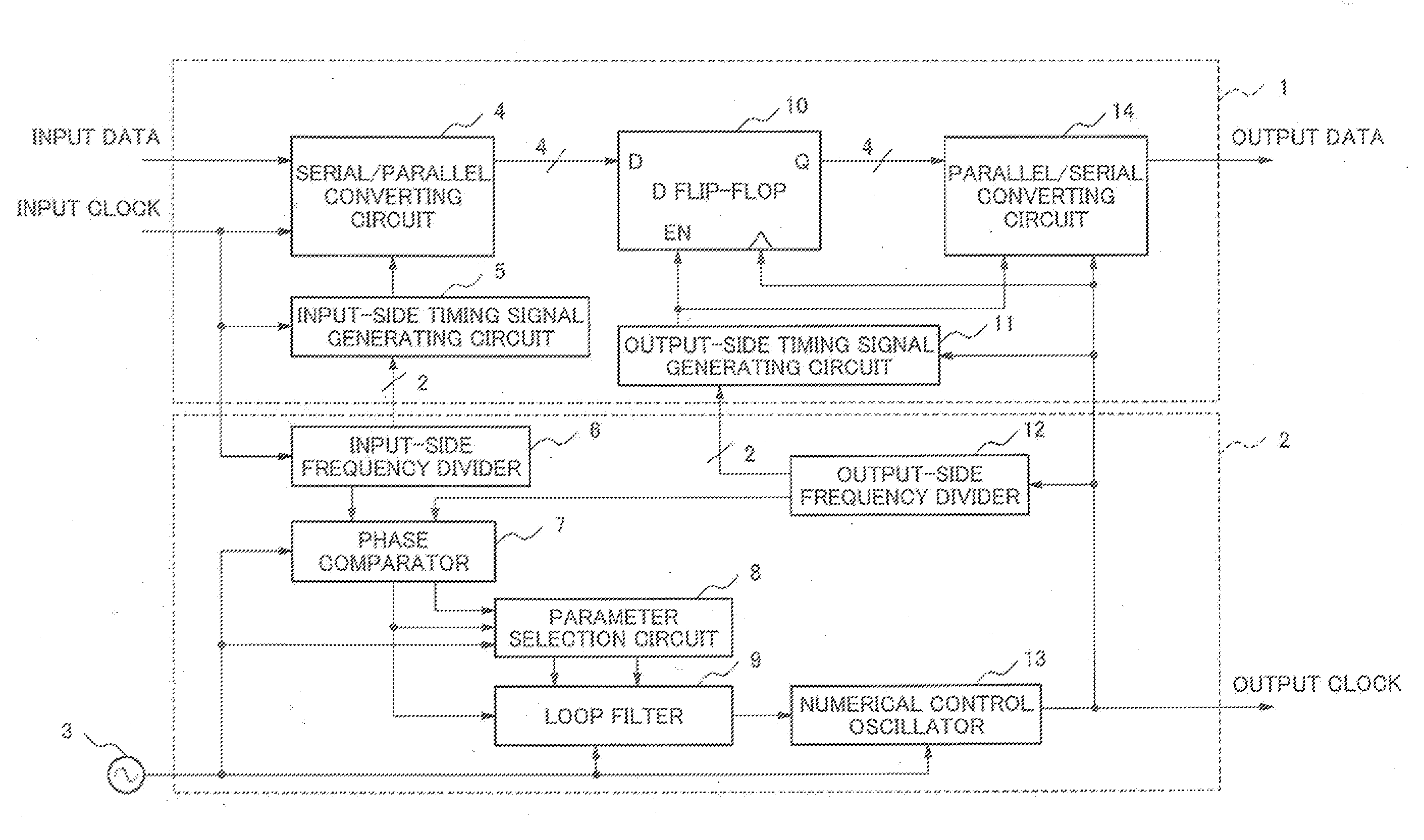
[0039]FIG. 1 is a block diagram which shows an example of a jitter suppression circuit according to the present invention.

[0040]A jitter suppression circuit shown in FIG. 1 includes a clock transferring part 1 and a digital phase locked loop (DPLL) 2 when separated generally.

[0041]The clock transferring part I includes a serial / parallel converting circuit 4, an input-side timing signal generating circuit 5, an output-side timing signal generating circuit 11, a D flip-flop 10 and a parallel / serial converting circuit 14. The DPLL 2 includes an input-side frequency divider 6, an output-side frequency divider 12, a phase comparator 7, a parameter selection circuit 8, a loop filter 9 and a numerical control oscillator 13. Each component of the clock transferring part 1 and the DPLL 2 will be described below.

[0042]First, “clock transferring” means “to change the operation clock of a flip-flop which performs retiming of data.” In FIG. 1, although up to the s...

example 2

[0105]A block diagram of another example of a jitter suppression circuit according to the present invention is shown in FIG. 13.

[0106]In FIG. 13, in the parameter selection circuit 8, output of the loop filter 9 is used as phase error information for synchronization determination. In comparison with the case where output of the phase comparator 7 is used for synchronization determination as is in a jitter suppression circuit shown in FIG. 1, because averaged phase error information is being used, more correct synchronization determination can be performed, although a quick parameter change cannot be performed.

[0107]A modified example of the loop filter 9 that is used in a jitter suppression circuit shown in FIG. 1 is shown in FIG. 14.

[0108]It is a digital filter with low pass characteristics like the case shown in FIG. 5, and its frequency characteristic is expressed in the formula (2). From the formula (2), it can be found out that, also by using the structure of FIG. 14, a bandwid...


PUM


Abstract

There is provided a jitter suppression circuit and a jitter suppression method in which both shortening of a pull-in time and high jitter suppression characteristics is satisfied.
In a jitter suppression circuit using a digital phase locked loop, both shortening of a pull-in time and high jitter suppression effect can be satisfied by determining whether the loop is in a synchronous state or not using a phase difference between an input clock and an output clock, and changing characteristics of a loop filter by the determination result.

Description

TECHNICAL FIELD[0001]The present invention relates to a jitter suppression circuit and a jitter suppression method.BACKGROUND ART [0002]In a digital transmission network, a pulse stuffing method is used for multiplexing asynchronous signals. In a pulse stuffing method, destuffing processing is needed in a receiving end. Because a signal for which destuffing processing has been performed has a large jitter, this jitter needs to be suppressed.[0003]Conventionally, as a suppression means of a destuffing jitter, as disclosed in patent document 1, a method using a memory and a digital phase locked loop (DPLL) has been formulated. In this method, a jitter included in input clock and input data can be suppressed by writing the input data in a memory once, reading the data from the memory using an output clock with less jitter, and then outputting it. Frequency synchronization is maintained between the input clock and the output clock by a DPLL so that the data discontinuity by the overflow...

Claims


Application Information

Patent Timeline
Patent Type & Authority Applications(United States)
IPC IPC(8): H03L7/093
CPCH03K5/1565H03L7/093H03L7/095H03L7/107H03L7/0991H03L7/1075
Inventor ADACHI, TAKAHIRO
Owner NEC CORP
Why Eureka
Try Eureka