Methods to fabricate a photoactive substrate suitable for microfabrication

a technology of photoactive substrates and microfabrication, which is applied in the direction of photomechanical equipment, instruments, originals for photomechanical treatment, etc., can solve the problems of long microfabrication process, difficult and expensive, and production silicon fabrication facilities costing millions mor

Active Publication Date: 2011-08-11
3D GLASS SOLUTIONS INC
View PDF19 Cites 81 Cited by
  • Summary
  • Abstract
  • Description
  • Claims
  • Application Information

AI Technical Summary

Benefits of technology

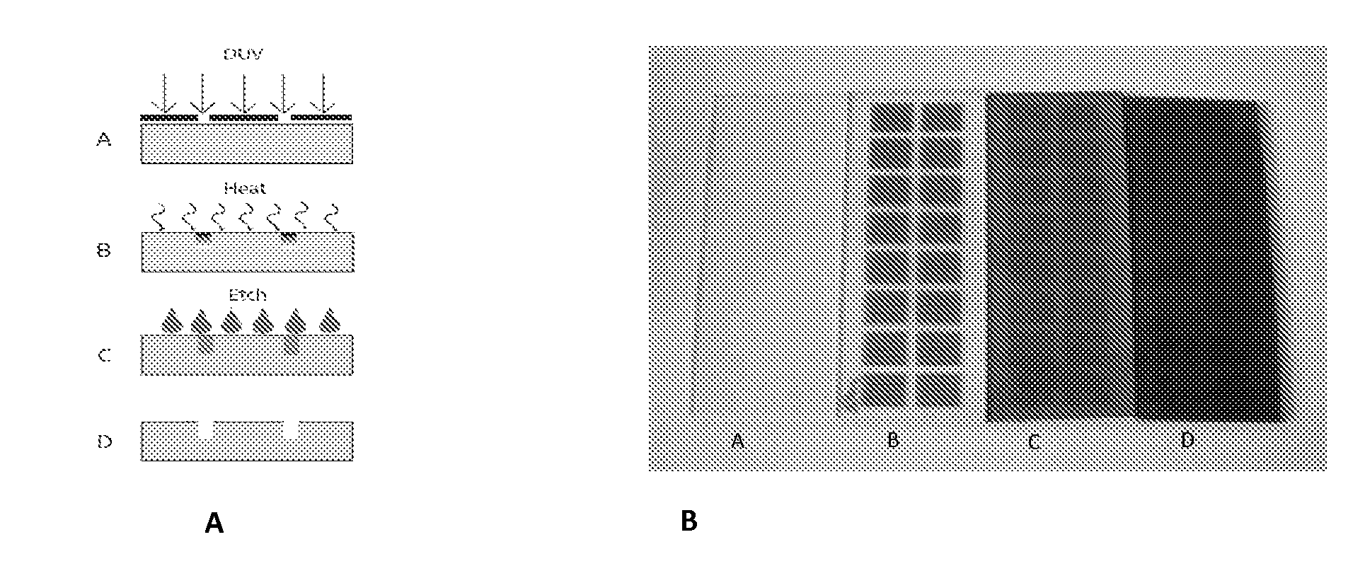
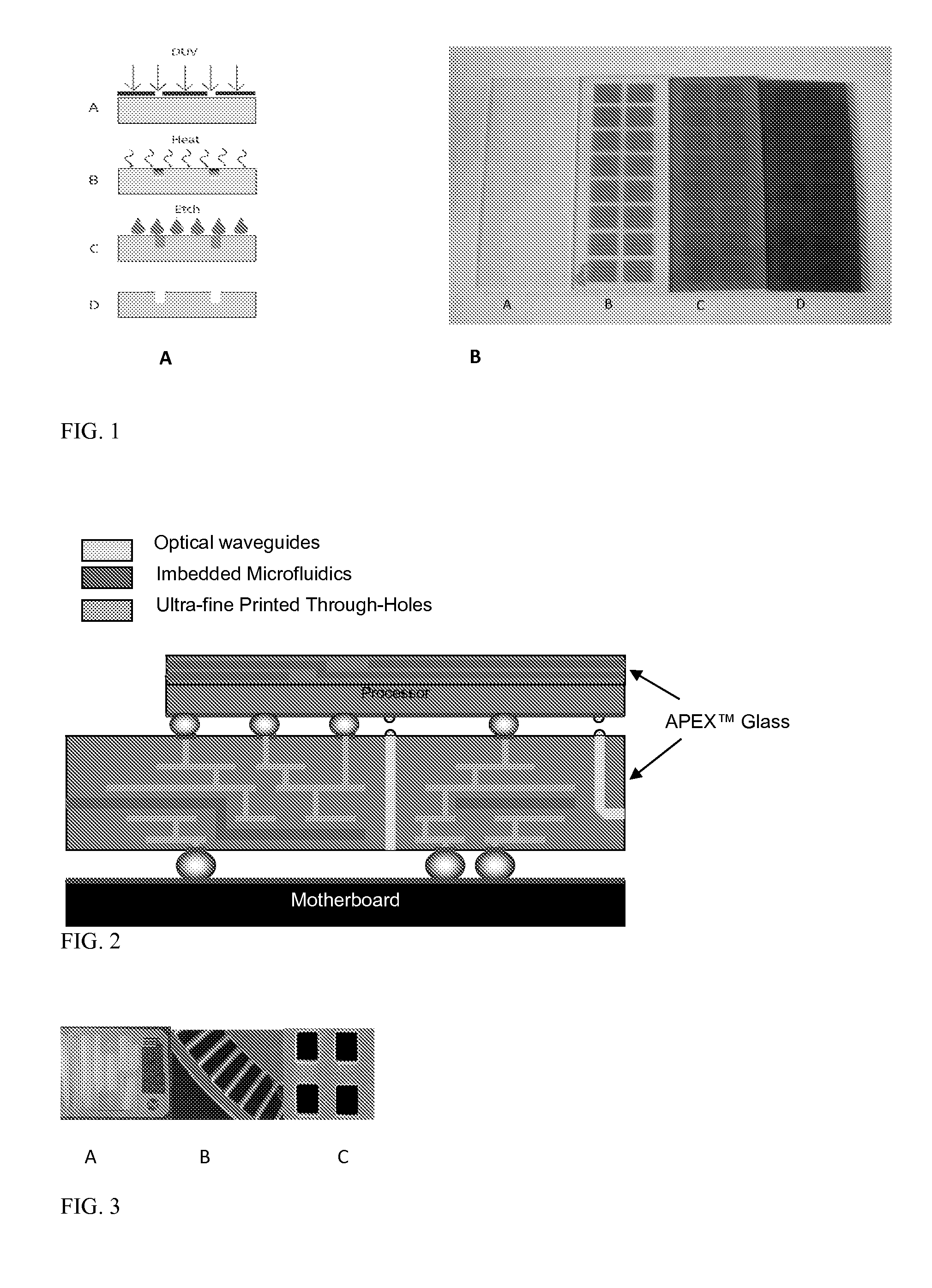
The present invention provides a way to make a special type of glass that can be used for transmitting light through it (called optical waves). This process involves creating small metals dots on the surface of the glass, then putting a pattern onto the glass which tells where the light should go. Next, the glass is baked very hot for several hours, causing some parts of it to turn into a solid state. Then, the rest of the glass is cooled down and shaped like a mirror. Finally, the finished product is washed with chemicals to remove any impurities. When this new glass is ready, it has tiny channels built inside it that allow light to pass through without being affected by other materials.

Problems solved by technology

The technical problem addressed by this patent is finding new ways to create photosensitive glass structures that can be used for various micro machinning and micro fabrication processes without requiring expensive and specialized equipment like traditional semiconductor assembly lines. This approach would make it easier and less expensive to develop products with small footprint sizes and advanced capabilities like heat dissipation or optical communication.

Method used


Image

  • Methods to fabricate a photoactive substrate suitable for microfabrication
  • Methods to fabricate a photoactive substrate suitable for microfabrication
  • Methods to fabricate a photoactive substrate suitable for microfabrication

Examples


Embodiment Construction

[0029]While the making and using of various embodiments of the present invention are discussed in detail below, it should be appreciated that the present invention provides many applicable inventive concepts that can be embodied in a wide variety of specific contexts. The specific embodiments discussed herein are merely illustrative of specific ways to make and use the invention and do not restrict the scope of the invention.

[0030]To facilitate the understanding of this invention, a number of terms are defined below. Terms defined herein have meanings as commonly understood by a person of ordinary skill in the areas relevant to the present invention. Terms such as “a”, “an” and “the” are not intended to refer to only a singular entity, but include the general class of which a specific example may be used for illustration. The terminology herein is used to describe specific embodiments of the invention, but their usage does not delimit the invention, except as outlined in the claims....


PUM

PropertyMeasurementUnit
Temperatureaaaaaaaaaa
Timeaaaaaaaaaa
Electric chargeaaaaaaaaaa

Abstract

A method of fabrication and device with holes for electrical conduction made by preparing a photosensitive glass substrate comprising at least silica, lithium oxide, aluminum oxide, and cerium oxide, masking a design layout comprising one or more holes to form one or more electrical conduction paths on the photosensitive glass substrate, exposing at least one portion of the photosensitive glass substrate to an activating energy source, exposing the photosensitive glass substrate to a heating phase of at least ten minutes above its glass transition temperature, cooling the photosensitive glass substrate to transform at least part of the exposed glass to a crystalline material to form a glass-crystalline substrate and etching the glass-crystalline substrate with an etchant solution to form the one or more depressions or through holes for electrical conduction in the device.

Description


Claims


Application Information

Patent Timeline
Owner 3D GLASS SOLUTIONS INC
Why Eureka
Try Eureka