Method of producing a silicon-on-sapphire type heterostructure

a heterostructure and silicon technology, applied in semiconductor/solid-state device manufacturing, basic electric elements, electric devices, etc., can solve the problems of increasing increasing the load of the wheel, and not being able to apply a very high load during grinding without risk, so as to limit the appearance of defects and the risk of delamination

Inactive Publication Date: 2011-08-11
S O I TEC SILICON ON INSULATOR THECHNOLOGIES
View PDF1 Cites 27 Cited by
  • Summary
  • Abstract
  • Description
  • Claims
  • Application Information

AI Technical Summary

Benefits of technology

[0017]One of the aims of the invention is to overcome the above-mentioned disadvantages by proposing a solution that can produce an SOS type heterostructure by bo...

Problems solved by technology

Because the bond between these two elements is weak (limitation on the temperature of the reinforcement anneal), it is not possible to apply a very high load with the wheel during grinding without risking delamination.
In contrast, with abrasive particles of smaller dimensions, corre...

Method used


Image

  • Method of producing a silicon-on-sapphire type heterostructure
  • Method of producing a silicon-on-sapphire type heterostructure
  • Method of producing a silicon-on-sapphire type heterostructure

Examples


Embodiment Construction

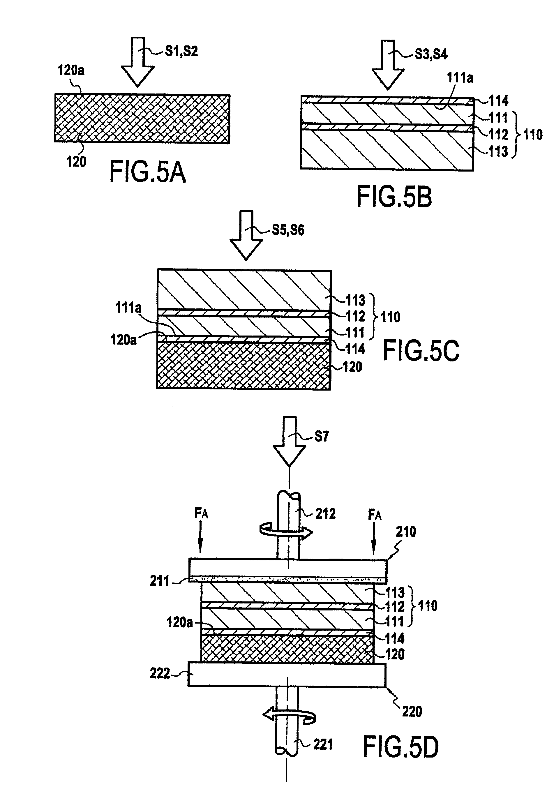
[0031]The method of the present invention is of general application to the production of an SOS type heterostructure formed from an assembly between a first substrate formed of sapphire and a second substrate, or SOI substrate. The substrates may, in particular, have diameters of 150 millimeters (mm).

[0032]Referring to FIGS. 5A to 5G and 6, a method of producing an SOS type heterostructure from an initial substrate 110 (top) and a support substrate 120 (base) is described.

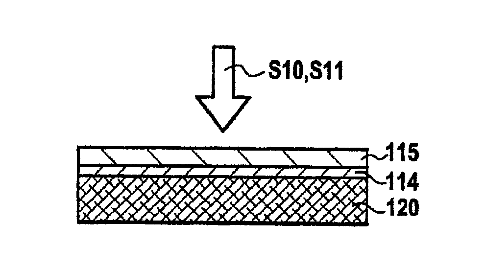
[0033]As can be seen in FIG. 5B, the initial substrate 110 is constituted by an SOI type structure comprising a layer of silicon 111 on a support 113, also of silicon, with a buried oxide layer 112, formed of SiO2, for example, being disposed between the layer 111 and the support 113.

[0034]The support substrate 120 is constituted by a wafer of sapphire (FIG. 5A).

[0035]Before carrying out bonding of the initial substrate 110 to the support substrate 120, the bonding surface 120a of the sapphire support substrate tha...


PUM


Abstract

The invention provides a method of producing a heterostructure of the silicon-on-sapphire type, comprising bonding an SOI substrate onto a sapphire substrate and thinning the SOI substrate, thinning being carried out by grinding followed by etching of the SOI substrate. In accordance with the method, grinding is carried out using a wheel with a grinding surface that comprises abrasive particles having a mean dimension of more than 6.7 μm; further, after grinding and before etching, the method comprises a step of post-grinding annealing of the heterostructure carried out at a temperature in the range of 150° C. to 170° C.

Description

CROSS-REFERENCE TO RELATED APPLICATIONS[0001]This is a national phase entry under 35 U.S.C. §371 of International Patent Application PCT / EP2009 / 065440, filed Nov. 19, 2009, published in English as International Patent Publication WO 2010 / 057941 A1 on May 27, 2010, which claims the benefit under Article 8 of the Patent Cooperation Treaty of French Patent Application Serial No. 0857954, filed Nov. 24, 2008, the entire disclosure of each of which is hereby incorporated herein by this reference.TECHNICAL FIELD[0002]The present invention relates to the production of heterogeneous structures formed by bonding at least one substrate of semiconductor material, such as silicon, on a sapphire (Al2O3) substrate. In particular, the invention is applicable to the fabrication of silicon-on-sapphire type heterostructures known by the acronym SOS (for silicon-on-sapphire).BACKGROUND[0003]Heterostructures comprising a layer of silicon on a sapphire substrate have particular advantages. SOS structure...

Claims


Application Information

Patent Timeline
IPC IPC(8): H01L21/762
CPCH01L21/76256H01L21/2007
Inventor GAUDIN, GWELTAZVAUFREDAZ, ALEXANDREGUITTARD, FLEUR
Owner S O I TEC SILICON ON INSULATOR THECHNOLOGIES
Why Eureka
Try Eureka