Light emitting device package and lighting system having the same
- Summary
- Abstract
- Description
- Claims
- Application Information
AI Technical Summary
Benefits of technology
Problems solved by technology
Method used
Image

Examples
first embodiment
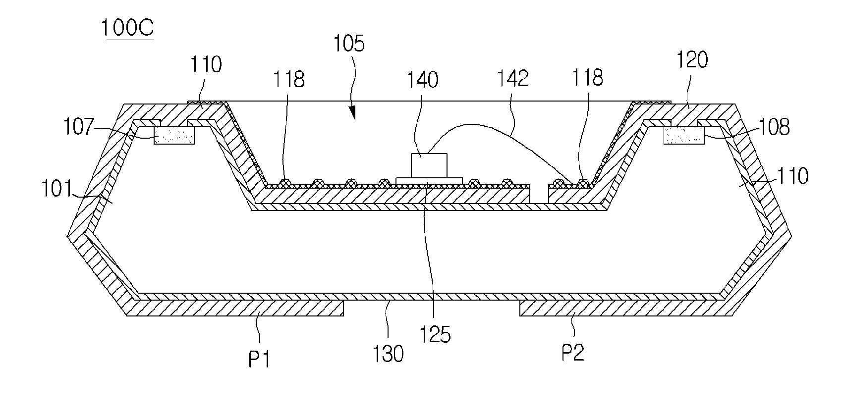
[0023]FIG. 1 is a plan view of a light emitting device package and FIG. 2 is a side sectional view taken along line A-A of FIG. 1.
[0024]Referring to FIGS. 1 and 2, the light emitting device package 100 includes a body 101, an insulating layer 130, first and second electrode layers 110 and 120, and a light emitting device 140.
[0025]The body 101 may include a silicon material. For instance, the body 10 may include wafer level package (WLP) having a silicon wafer. The body 101 can be formed by using Al, AlN, AlOx, PSG (photo sensitive glass), Al2O3, BeO, PCB (Printed Circuit Board) or various resins in addition to the silicon. According to the embodiment, the silicon is used as a material for the body 101 to improve the manufacturing efficiency and the heat dissipation efficiency of the light emitting device package.
[0026]The body 101 can be formed through the bulk etching process, such as wet etching, dry etching or laser drilling. At least two of the above etching processes can be p...
second embodiment
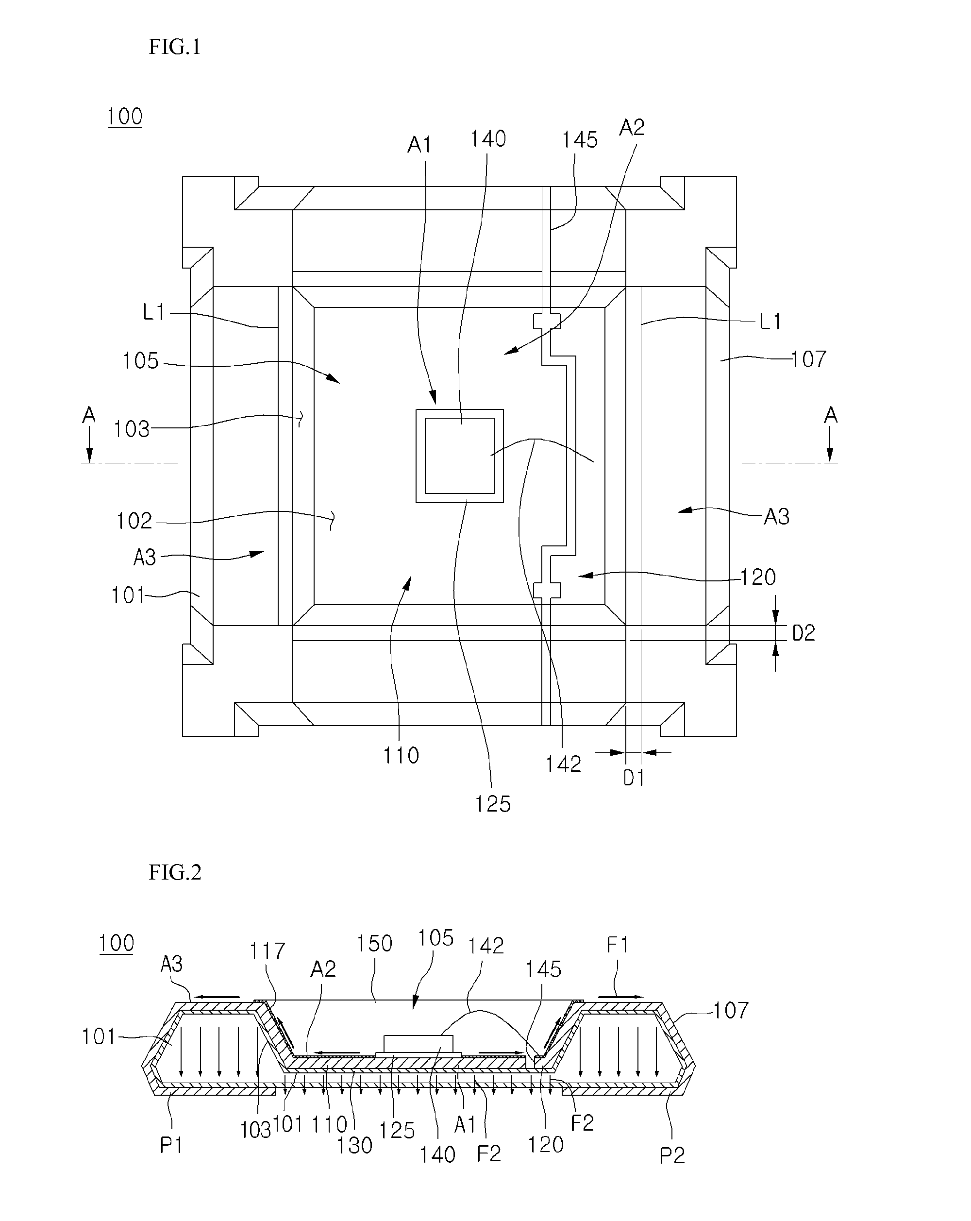
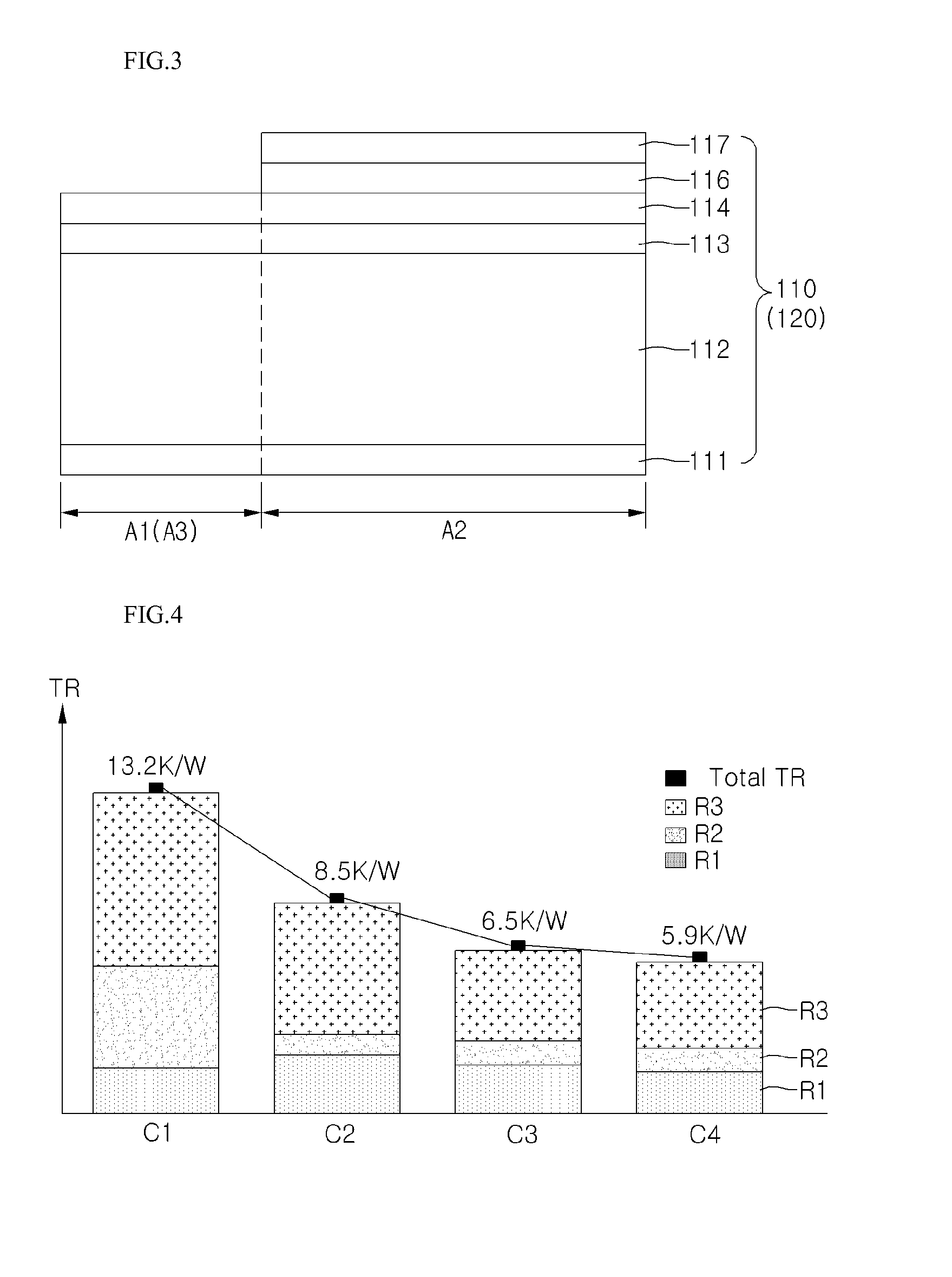
[0106] the thermal diffusion layer 112 as shown in FIG. 3 is formed in formed in the electrode layers 110 and 120, so that the effective heat dissipation area and the thermal conductive area are increased, thereby lowering the thermal resistance of the package. In addition, the first thermal flow F1 flowing in the horizontal direction is greater than the second thermal flow F2 flowing in the vertical direction, so that the heat dissipation efficiency of the package can be improved.
[0107]FIG. 6 is a sectional view showing a light emitting device package according to the third embodiment. In the following description of the third embodiment, the elements and structures the same as those of the first embodiment will be referred to the first embodiment and detailed description thereof will be omitted in order to avoid redundancy.
[0108]Referring to FIG. 6, the light emitting device package 100B includes a body 101A having a flat top surface, an insulating layer 130, a plurality of electr...
PUM
 Abstract
Description
Claims
Application Information
 - Generate Ideas
- Intellectual Property
- Life Sciences
- Materials
- Tech Scout
- Unparalleled Data Quality
- Higher Quality Content
- 60% Fewer Hallucinations
Browse by: Latest US Patents, China's latest patents, Technical Efficacy Thesaurus, Application Domain, Technology Topic, Popular Technical Reports.
© 2025 PatSnap. All rights reserved.Legal|Privacy policy|Modern Slavery Act Transparency Statement|Sitemap|About US| Contact US: help@patsnap.com