Wiring board and liquid crystal display device

a liquid crystal display and wiring board technology, applied in the field of wiring boards, can solve problems such as leakage failure and leakage failure, and achieve the effect of reducing the risk of leakage failur

Active Publication Date: 2011-08-18
SHARP KK
View PDF9 Cites 15 Cited by
  • Summary
  • Abstract
  • Description
  • Claims
  • Application Information

AI Technical Summary

Benefits of technology

[0059]This allows for production of a wiring board and a liquid crystal display dev...

Problems solved by technology

The arrangement of Patent Literature 1 unfortunately tends to cause a problem of a leak failure between a pad 109 and a metal wire 101 when an electronic component such as a driving IC ...

Method used


Image

  • Wiring board and liquid crystal display device
  • Wiring board and liquid crystal display device
  • Wiring board and liquid crystal display device

Examples


embodiment

PRESENT EMBODIMENT

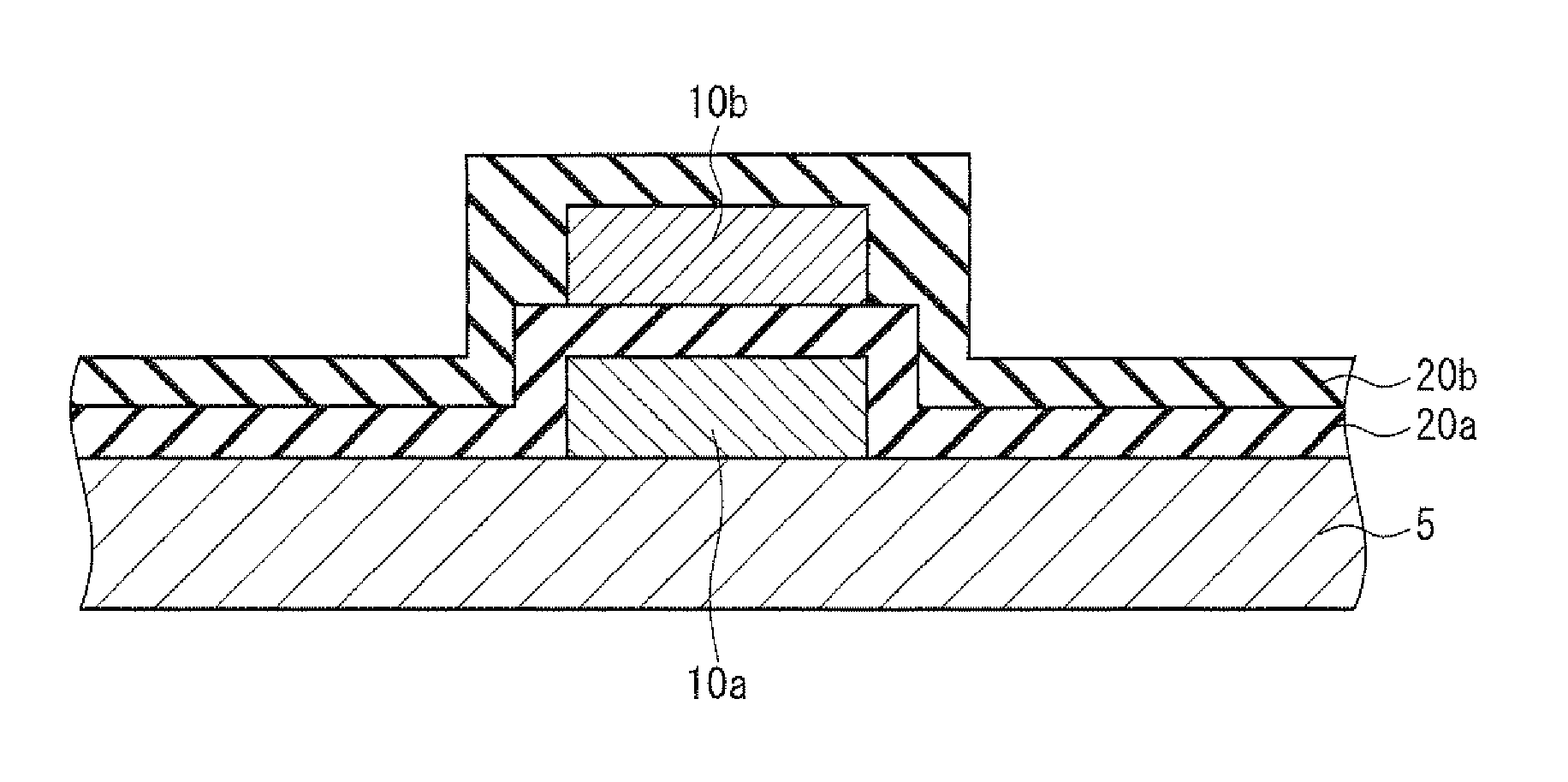
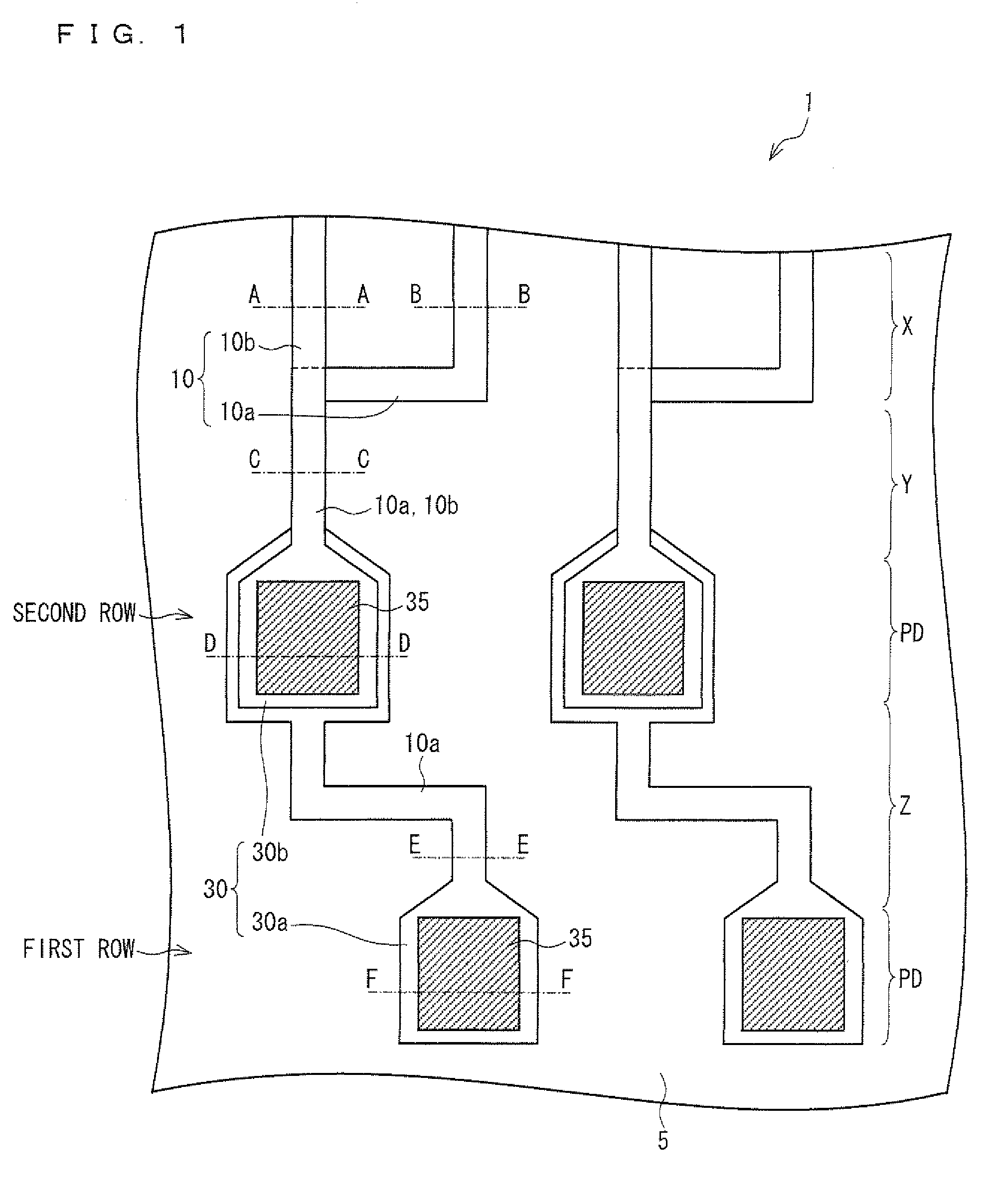
[0147]In contrast, according to the wiring board 1 of the present embodiment, while first metal wires 10a each connected to a first-row pad 30a and second metal wires 10b each connected to a second-row pad 30b are provided in a single layer on the substrate 5 in a drawing region (region X illustrated in FIG. 1), the first and second metal wires 10a and 10b are provided in separate layers in a second connection region (region Y illustrated in FIG. 1), in which the second metal wires 10b are connected to the corresponding second-row pads 30b.

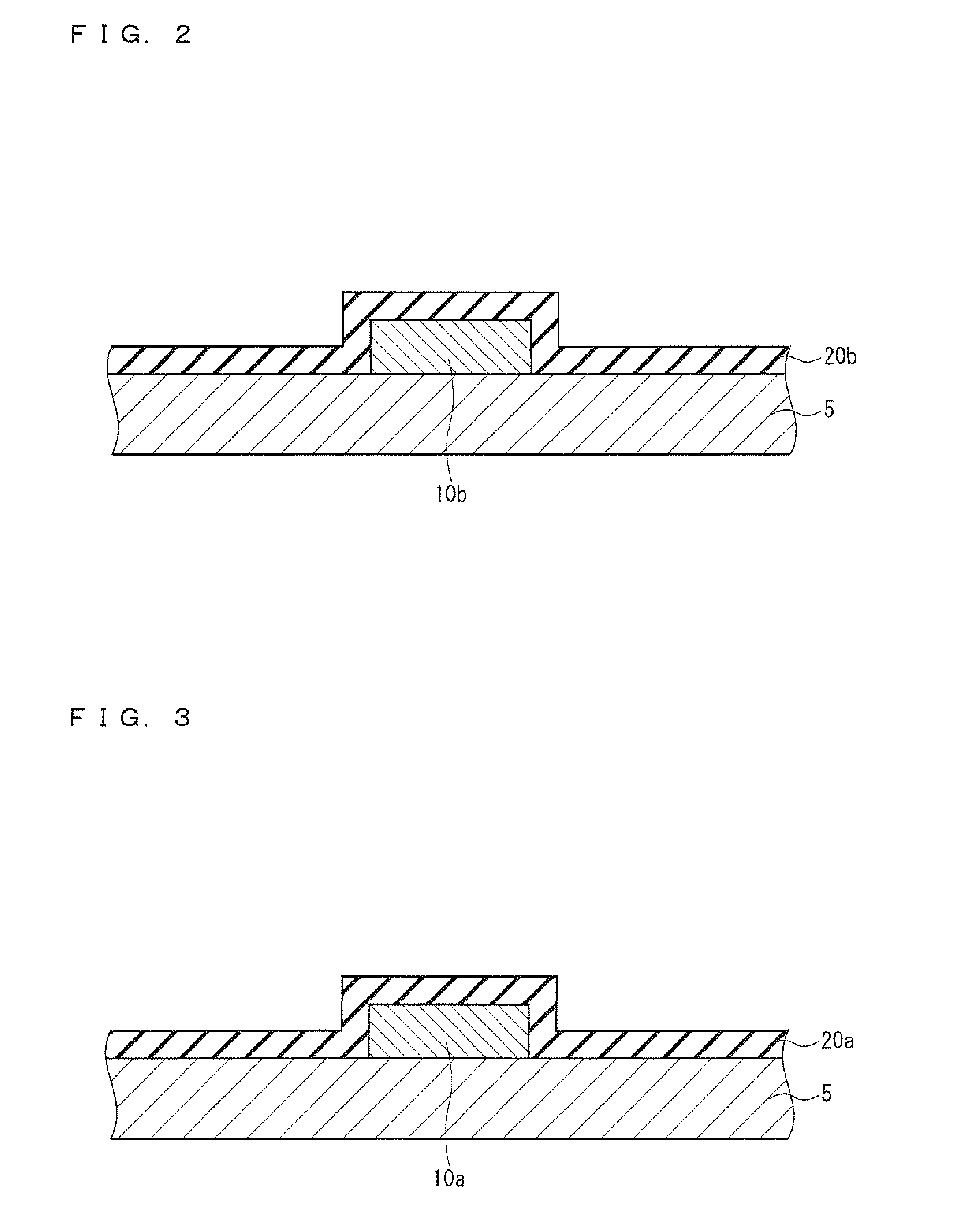
[0148]More specifically, as illustrated in FIGS. 2 and 3, the first and second metal wires 10a and 10b are, although made of different materials as described below, provided in a single layer on the substrate 5 in the drawing region X. Further, the first and second metal wires 10a and 10b are covered with first and second insulating layers 20a and 20b, respectively.

[0149]FIG. 2 is a cross-sectional view (taken along line A-A of ...


PUM


Abstract

A wiring board of the present invention (1) is arranged so that: pads (30) arranged in a plurality of rows include: first-row pads (30a) connected to first metal wires (10a) among metal wires (10); and second-row pads (30b) connected to second metal wires (10b) among the metal wires (10), the first metal wires (10a) being longer than the second metal wires (10b); each of the first metal wires (10a) is formed so as to be separated from a corresponding one of the second-row pads (30b) by at least an insulating layer, and so as to have a widthwise center in a lower region below the corresponding second-row pad (30b); and each of the first metal wires (10a) has widthwise edges provided, in a plan view, beyond widthwise edges of a corresponding one of the second-row pads (30b) in a region in which the first metal wire (10a) overlaps with the corresponding second-row pad (30b).

Description

TECHNICAL FIELD[0001]The present invention relates to a wiring board. In particular, the present invention relates to a wiring board having pads arranged in a plurality of rows and to a liquid crystal display device including such a wiring board.BACKGROUND ART[0002]Conventionally, there has been widely used a wiring board having pads arranged in a so-called plurality of rows for a narrow-pitch mounting.[0003]In view of a demand for further reduction in size and weight of electronic devices including the wiring board, electronic components in each of such electronic devices are mounted at a higher density. Accordingly, the wiring board on which the electronic components are mounted are required to have a narrower pitch.[0004](Patent Literature 1)[0005]In order to meet such a demand, various techniques have been suggested. Patent Literature 1, for example, discloses a technique to arrange a wiring board having pads provided in a plurality of rows. In the technique, the pads are provid...

Claims


Application Information

Patent Timeline
IPC IPC(8): G02F1/1345H05K1/11H01L23/532
CPCG02F1/1345H01L2224/16225G02F2001/13629H01L2924/01013H01L2924/01022H01L2924/01033H01L2924/01046H01L2924/01049H01L2924/01073H01L2924/01082H01L2924/04941H01L2924/04953H01L2924/14H05K1/111H05K1/117H05K3/4644H05K2201/09672H05K2201/09709H01L2924/01005H01L2924/01006H01L2924/01019H01L2224/17155H01L2224/16227H01L2924/00013G02F1/13458H01L2224/13099H01L2224/13599H01L2224/05599H01L2224/05099H01L2224/29099H01L2224/29599Y02P70/50G02F1/13629
Inventor MATSUI, TAKASHISHIOTA, MOTOJI
Owner SHARP KK
Why Eureka
Try Eureka