Corner layout for superjunction device

a superjunction and junction technology, applied in semiconductor devices, instruments, computing, etc., can solve the problems of high cost of use of such software, low breakdown voltage of straight ends of p-columns, and inability to clamp inductively, so as to achieve easy charge balance

Active Publication Date: 2011-08-25
ALPHA & OMEGA SEMICON INC
View PDF2 Cites 51 Cited by
  • Summary
  • Abstract
  • Description
  • Claims
  • Application Information

AI Technical Summary

Benefits of technology

[0039]There can be some flexibility in determining the shapes of the regions p1, n1, p2, n2, p3 and n3. The sizes, shapes and location of the implanted areas p1, p2 and p3 can be determined using the result from equation (6).
[0040]It should be noted that most parts of the active cell P-type columns such as 204 and 206 are straight and run parallel to one anot

Problems solved by technology

A superjunction MOSFET device with a curved corner design and straight ends to the P-columns will often exhibit a low breakdown voltage due to charge imbalance in the corner regions.
Unfortunately, such

Method used


Image

  • Corner layout for superjunction device
  • Corner layout for superjunction device
  • Corner layout for superjunction device

Examples


Embodiment Construction

[0017]Although the following detailed description contains many specific details for the purposes of illustration, one of ordinary skill in the art will appreciate that many variations and alterations to the following details are within the scope of the invention. Accordingly, the exemplary embodiments of the invention described below are set forth without any loss of generality to, and without imposing limitations upon, the claimed invention.

INTRODUCTION

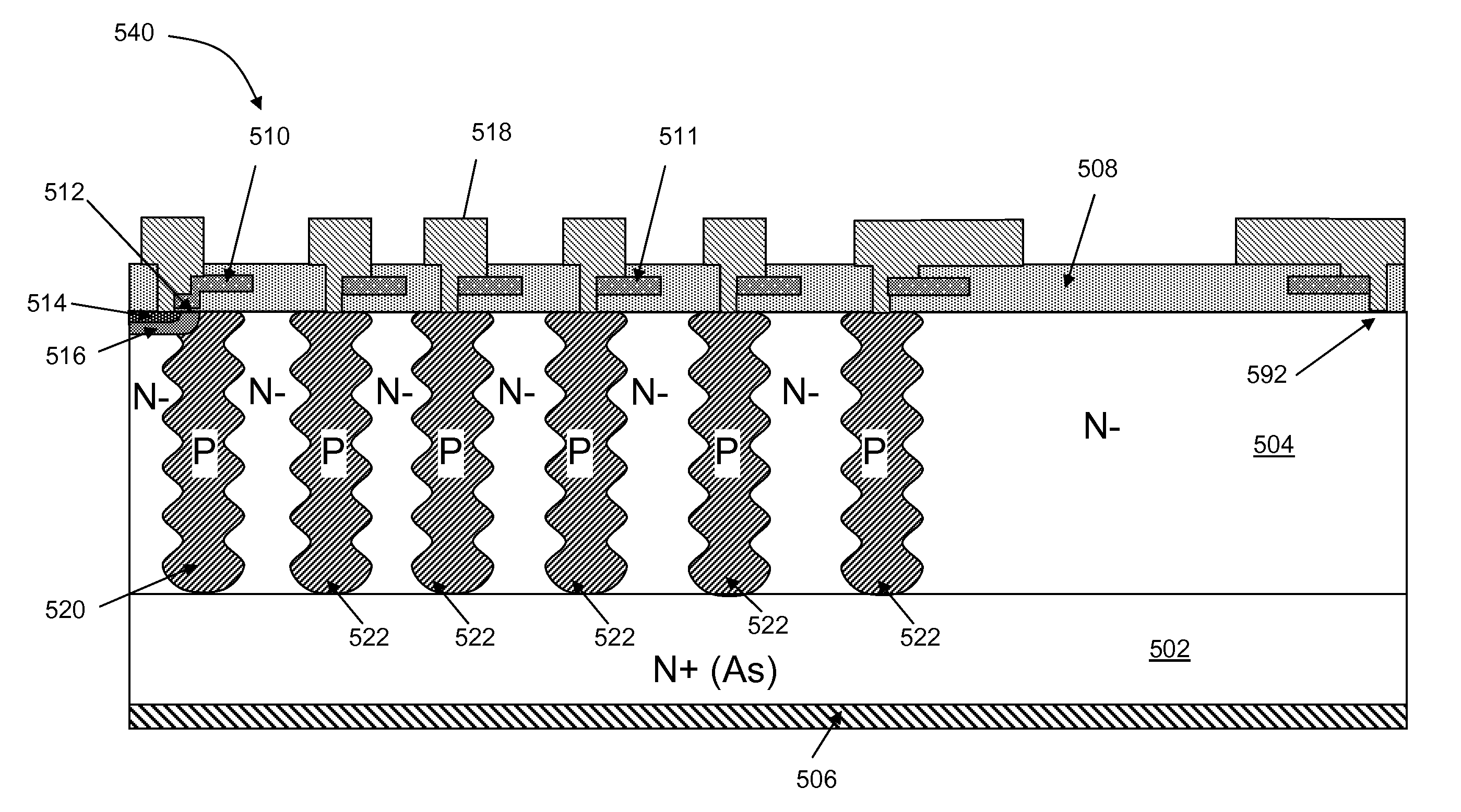
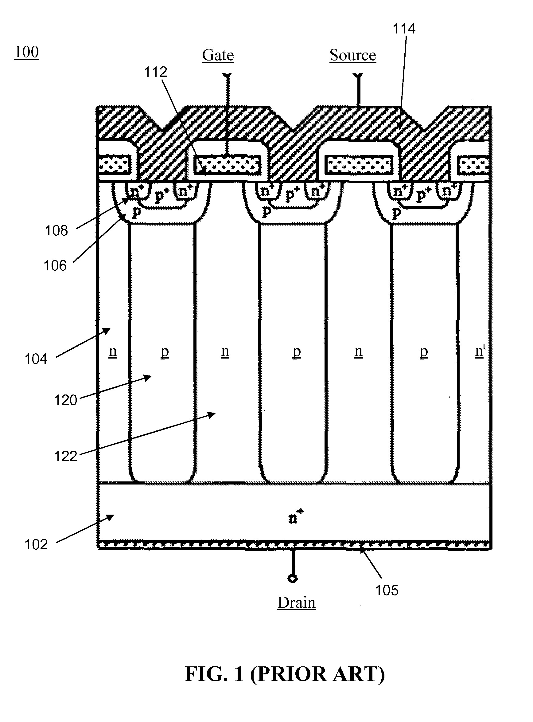
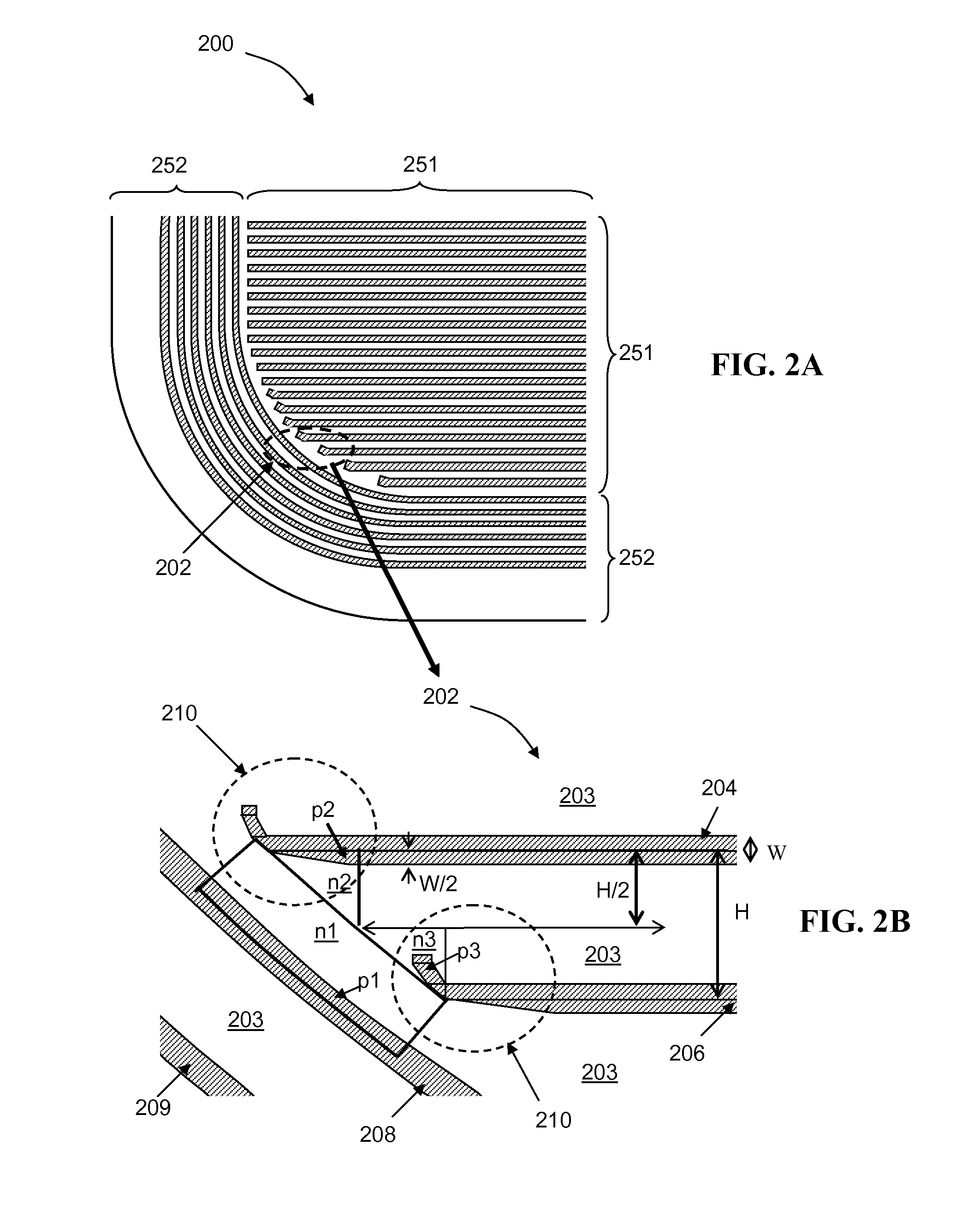
[0018]A superjunction MOSFET device with a curved corner design and straight ends to the P-columns will often exhibit a low breakdown voltage due to charge imbalance in the corner regions. Prior attempts have been made to balance the charge in the corner region by leaving small holes or P column islands that are not connected in main P column strip. Unfortunately, such solutions can cause problems with unclamped inductive switching (UIS) or might not provide enough a large improvement in BV. In addition, many approaches to charge ba...


PUM


Abstract

A superjunction device and methods for layout design and fabrication of a superjunction device are disclosed. A layout of active cell column structures can be configured so that a charge due to first conductivity type dopants balances out charge due to second conductivity type dopants in a doped layer in an active cell region. A layout of end portions of the active cell column structures proximate termination column structures can be configured so that a charge due to the first conductivity type dopants in the end portions and a charge due to the first conductivity type dopants in the termination column structures balances out charge due to the second conductivity type dopants in a portion of the doped layer between the termination column structures and the end portions.

Description

FIELD OF THE INVENTION[0001]This invention generally relates to metal oxide semiconductor field effect transistors (MOSFETs) and more particularly to a termination structure for a superjunction type MOSFET device.BACKGROUND OF THE INVENTION[0002]Power MOSFETs have typically been developed for applications requiring power switching and power amplification. For power switching applications, the commercially available devices are typically double diffused MOSFETs (DMOSFETs). In a typical transistor, much of the breakdown voltage BV is supported by a drift region, which is lowly doped in order to provide a higher breakdown voltage BV. However, the lowly doped drift region also produces high on-resistance Rds-on. For a typical transistor, Rds-on is proportional to BV2.5. Rds-on therefore increases dramatically with increase in breakdown voltage BV for a conventional transistor.[0003]Superjunctions are a well known type of semiconductor device. Superjunction transistors provide a way to a...

Claims


Application Information

Patent Timeline
IPC IPC(8): H01L29/78G06F17/50H01L29/06
CPCH01L29/0634H01L29/0638H01L29/0696H01L29/1095H01L29/7823H01L29/404H01L29/47H01L29/7811H01L29/402
Inventor GUAN, LINGPENGBHALLA, ANUPZHU, TINGGANGBOBDE, MADHUR
Owner ALPHA & OMEGA SEMICON INC
Why Eureka
Try Eureka