Method and System for Implementing High-Speed Interfaces Between Semiconductor Dies in Optical Communication Systems

a technology of optical communication system and semiconductor die, applied in the field of signal processing, can solve the problems of cable bulk penalty, large power consumption, complex structure, etc., and achieve the effect of small improvement in reach and limited scalability

Active Publication Date: 2011-08-25
CISCO TECH INC
View PDF9 Cites 20 Cited by
  • Summary
  • Abstract
  • Description
  • Claims
  • Application Information

AI Technical Summary

Benefits of technology

[0014]FIG. 5. is a block diagram illustrating a low-impedance split-transm

Problems solved by technology

They can be mitigated to some extent with equalization, coding, and shielding, but these techniques require considerable

Method used


Image

  • Method and System for Implementing High-Speed Interfaces Between Semiconductor Dies in Optical Communication Systems
  • Method and System for Implementing High-Speed Interfaces Between Semiconductor Dies in Optical Communication Systems
  • Method and System for Implementing High-Speed Interfaces Between Semiconductor Dies in Optical Communication Systems

Examples


Embodiment Construction

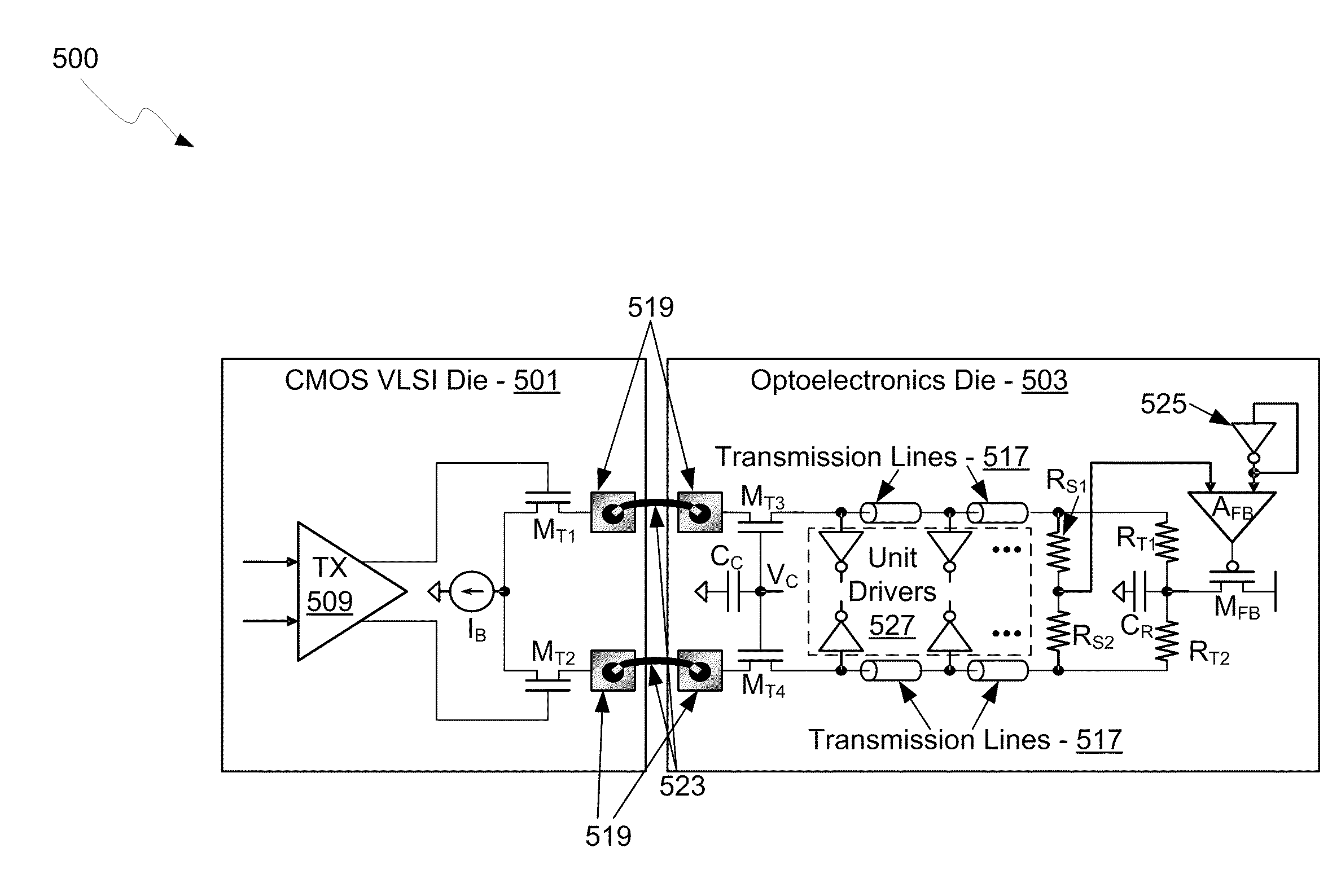
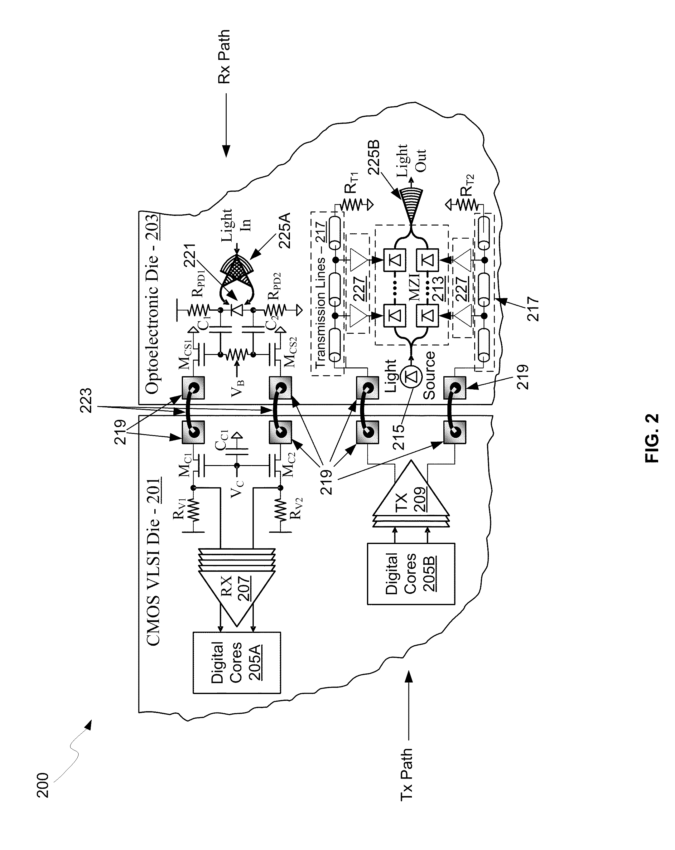
[0015]Certain aspects of the invention may be found in a method and system for implementing high-speed electrical interfaces between semiconductor dies in optical communication systems. Exemplary aspects of the invention may comprise communicating electrical signals between an electronics die and an optoelectronics die via coupling pads on the electronics die and the optoelectronics die in an optical communication system. The coupling pads may be located at low impedance points in one or more transmit paths and / or one or more receive paths in the optical communication system. The electrical signals may be communicated via one or more current-mode interfaces that may comprise a cascode amplifier stage split between source terminals of transistors on the electronics die and drain terminals of transistors on the optoelectronics die. The electrical signals may be communicated via one or more controlled-impedance interfaces that may comprise one or more transmission line drivers on a fir...


PUM


Abstract

A method and system for implementing high-speed electrical interfaces between semiconductor dies in optical communication systems are disclosed and may include communicating electrical signals between an electronics die and an optoelectronics die via coupling pads which may be located in low impedance points in Tx and Rx paths. The electrical signals may be communicated via one or more current-mode, controlled impedance, and/or capacitively-coupled interfaces. The current-mode interface may include a cascode amplifier stage split between source and drain terminals of transistors on the dies. The controlled-impedance interfaces may include transmission line drivers on a first die and transmission lines on a second die. The capacitively-coupled interfaces may include capacitors formed by contact pads on the dies. The coupling pads may be connected via one or more of: wire bonds, metal pillars, solder balls, or conductive resin. The dies may comprise CMOS and may be coupled in a flip-chip configuration.

Description

CROSS-REFERENCE TO RELATED APPLICATIONS / INCORPORATION BY REFERENCE[0001]This application makes reference to and claims priority to U.S. Provisional Application Ser. No. 61 / 338,690 filed on Feb. 23, 2010, which is hereby incorporated herein by reference in its entirety.FEDERALLY SPONSORED RESEARCH OR DEVELOPMENT[0002][Not Applicable]MICROFICHE / COPYRIGHT REFERENCE[0003][Not Applicable]FIELD OF THE INVENTION[0004]Certain embodiments of the invention relate to signal processing. More specifically, certain embodiments of the invention relate to a method and system for implementing high-speed electrical interfaces between semiconductor dies in optical communication systems.BACKGROUND OF THE INVENTION[0005]As data networks scale to meet ever-increasing bandwidth requirements, the shortcomings of copper data channels are becoming apparent. Signal attenuation and crosstalk due to radiated electromagnetic energy are the main impediments encountered by designers of such systems. They can be mi...

Claims


Application Information

Patent Timeline
IPC IPC(8): G02B6/26
CPCG02B6/4286G02B6/4274
Inventor KUCHARSKI, DANIELGUCKENBERGER, JOHN ANDREWPINGUET, THIERRYABDALLA, SHERIF
Owner CISCO TECH INC
Why Eureka
Try Eureka