
Semiconductor light-emitting element, method of manufacturing same, and light-emitting device

a technology of semiconductors and light-emitting elements, which is applied in the direction of semiconductor/solid-state device manufacturing, semiconductor devices, electrical devices, etc., can solve the problems of low light-emission efficiency, low yield, and variation in light-emission efficiency, and achieve the effect of increasing the emission efficiency of mixed colors

Inactive Publication Date: 2011-09-08
PANASONIC CORP
View PDF2 Cites 7 Cited by
  • Summary
  • Abstract
  • Description
  • Claims
  • Application Information

AI Technical Summary

Benefits of technology

[0015]With the foregoing in view, it is an object of the present invention to provide a semiconductor light-emitting element with increased light emission efficiency and a method of manufacturing the semiconductor light-emitting element.

Problems solved by technology

However in this case, it is necessary to maintain the electric conductivity and bonding strength, therefore, the yield drops and the productivity decreases.
Therefore, the size and density of pyramidal protrusions strongly depend on such as crystallinity of the n-type GaN film 22′, reproducibility of size and density of the pyramidal protrusions is low, and the light extraction efficiency causes a variation, therefore the light-emission efficiency causes a variation, and cost is increased due to drop of the yield.
Therefore, the light emission efficiency is difficult to increase.
The resultant problem is that the light emission efficiency is low.

Method used


Image

  • Semiconductor light-emitting element, method of manufacturing same, and light-emitting device
  • Semiconductor light-emitting element, method of manufacturing same, and light-emitting device
  • Semiconductor light-emitting element, method of manufacturing same, and light-emitting device

Examples


embodiment 1

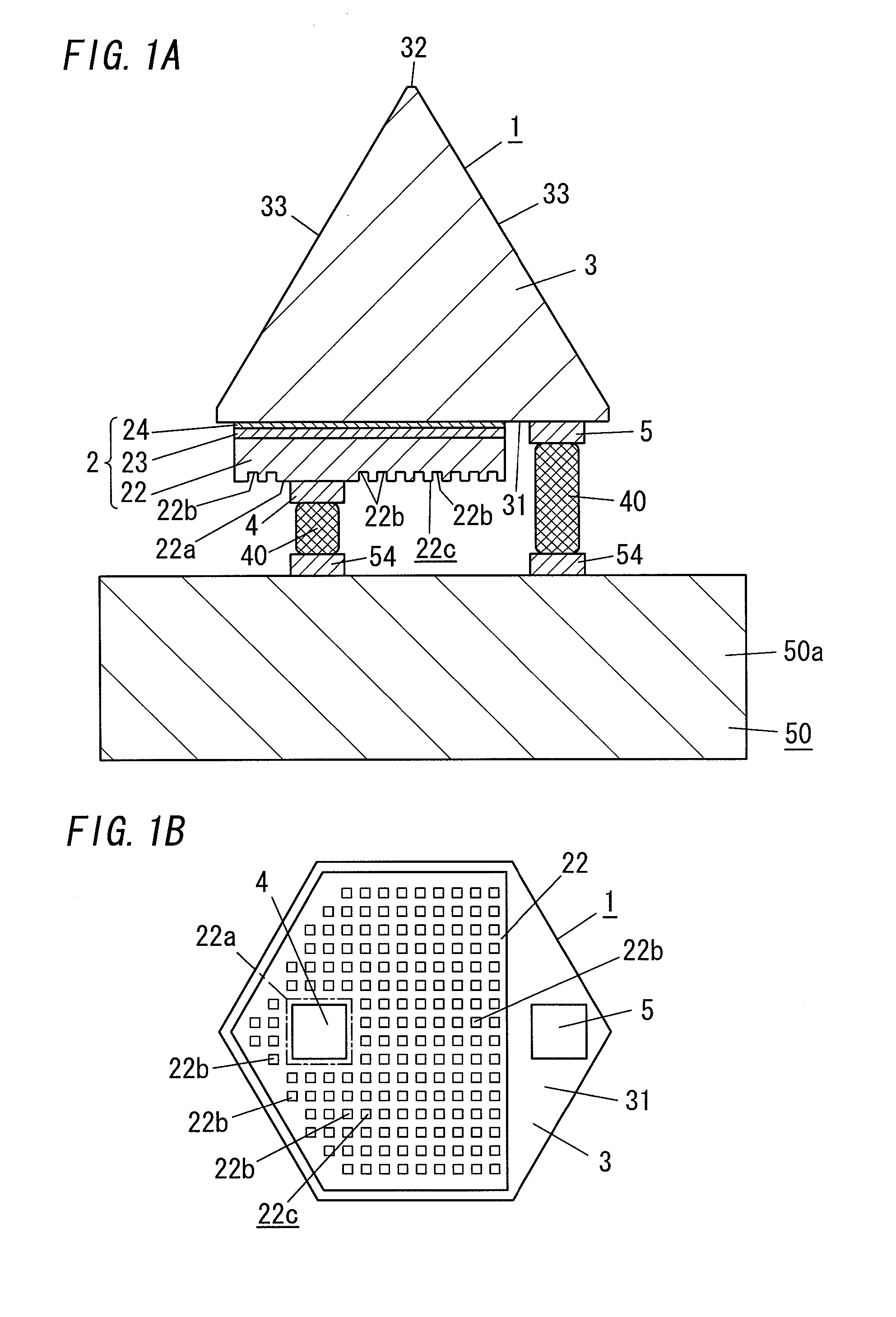
[0036]A semiconductor light-emitting element 1 according to the present embodiment will be described below with reference to FIG. 1.

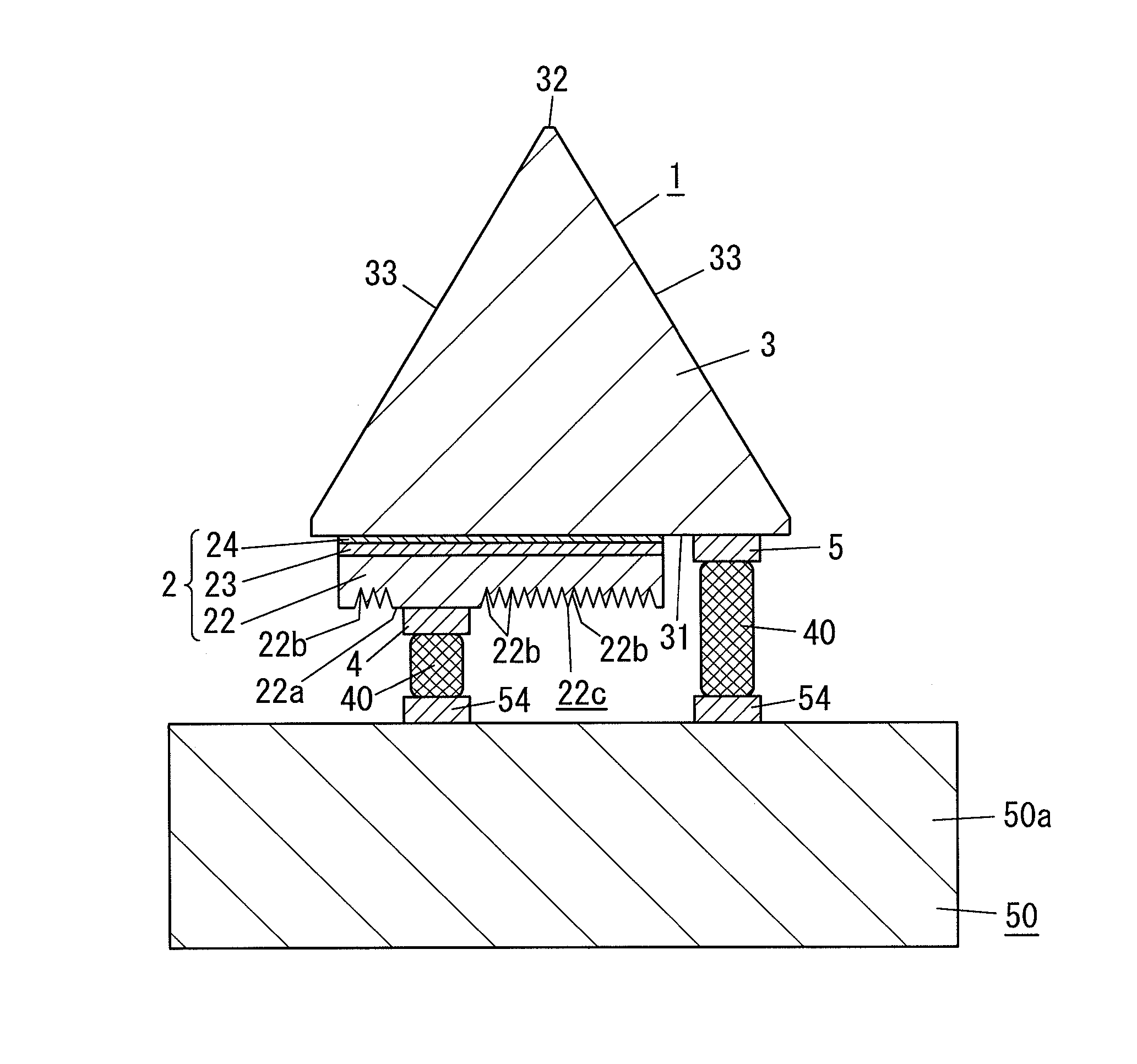
[0037]The semiconductor light-emitting element 1 according to the present embodiment is provided with a light-emitting layer 2 that is a blue LED chip of a GaN system emitting blue light, a conductive base 3 formed from n-type ZnO, a cathode 4, and an anode 5. The light-emitting layer 2 has an n-type GaN film 22 and a p-type GaN film 24. The base 3 is formed in a hexagonal pyramidal shape and has a bottom surface 31 that is directly joined to the light-emitting layer 2. The cathode 4 is formed to be in ohmic contact with the lower surface of the n-type GaN film 22 which is an N-polar plane. The anode 5 is formed to be in ohmic contact with the base 3.

[0038]In the semiconductor light-emitting element 1 according to the present embodiment, the light-emitting layer 2 has a laminated structure including the n-type GaN film 22, a light-emitting film 23, and ...

embodiment 2

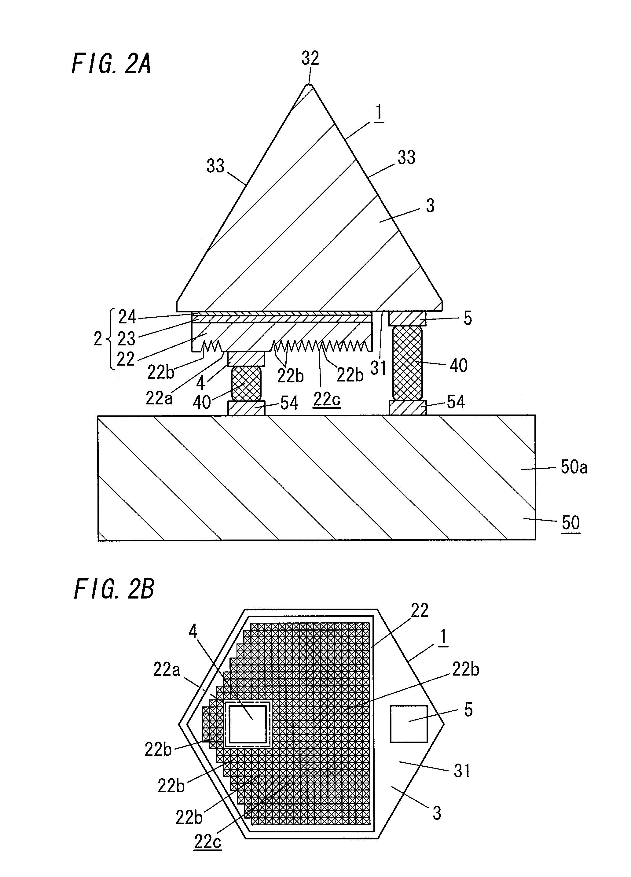
[0060]The basic structures of the semiconductor light-emitting element 1 and the light-emitting device according to the present embodiment that are shown in FIG. 2 and FIG. 3 are substantially identical to those of Embodiment 1 and only the shape of the fine peak-valley structure 22c is different. The constituent elements similar to those of Embodiment 1 are denoted with same reference numerals and explanation thereof is herein omitted.

[0061]The lower surface of the n-type GaN film 22 in the present embodiment has the flat portion 22a, which is the N-polar plane where the cathode electrode 4 has been formed, and the fine peak-valley structure 22c. The inner side surfaces of the recesses 22b constituting the fine peak-valley structure 22c are inclined surfaces with an inclination angle θ of less than 90 degrees with respect to the plane including the N-polar plane. Thus, the recess 22b is formed such that the opening diameter thereof increases gradually toward the N-polar plane of th...

embodiment 3

[0066]The basic structures of the semiconductor light-emitting element 1 and the light-emitting device according to the present embodiment that are shown in FIG. 5 are substantially identical to those of Embodiment 2, and only the shape of the fine peak-valley structure 22c (inclination angle θ shown in FIG. 3) and the number of flat portions 22a of the n-type GaN film 22, the number of the cathodes 4, and the number of the anodes 5 (in the present embodiment, two of each) are different. The constituent elements similar to those of Embodiment 2 are denoted with same reference numerals and explanation thereof is herein omitted.

[0067]In the semiconductor light-emitting element 1 according to the present embodiment, the cathode 4 and the anode 5 are constituted by a laminated film of an Al film and a Au film. The thickness of the Al film is set to 100 nm and the thickness of the Au film is set to 500 nm. These thicknesses are not particularly limited. The laminated films of the cathode...


PUM


Abstract

A semiconductor light-emitting element, a method of manufacturing same, and a light-emitting device enabling an increase in light emission efficiency is provided. The semiconductor light-emitting element 1 in accordance with the present invention includes: a light-emitting layer 2 having a laminated structure in which a p-type GaN film 24 and an n-type GaN film 22 are included; a conductive hexagonal pyramidal base 3 formed from ZnO and mounting with the light-emitting layer on a bottom surface 31; an anode 5 joined to the bottom surface 31 of the base 3 at a position apart from the light-emitting layer 2; and a cathode 4 mounted on the light-emitting layer 2. In the semiconductor light-emitting element 1, the p-type GaN film 24 is joined to the bottom surface 31 of the base 3, and the cathode 4 is joined to an N-polar plane of the n-type GaN film 22, said N-polar plane of the n-type GaN film 22 being an opposite side to the p-type GaN film 24. In the semiconductor light-emitting element 1, the N-polar plane of the n-type GaN film 22 has a fine peak-valley structure 22c outside a portion joined to the cathode 4.

Description

TECHNICAL FIELD[0001]The present invention relates to a semiconductor light-emitting element, a method of manufacturing same, and a light-emitting device.BACKGROUND ART[0002]Research and development aimed at increase in efficiency and output of semiconductor light-emitting elements including a LED chip in which a light-emitting layer is formed from a nitride semiconductor material (GaN, InGaN, AlGaInN, etc.) have been heretofore widely conducted. Research and development of light-emitting devices emitting mixed color light with a different color from that of an emission color of semiconductor light-emitting elements have also been widely conducted by combining the semiconductor light-emitting elements of this type with fluorescent materials, and abundant research and development have been performed to expand the application of such light-emitting devices to a general illumination field. Such light-emitting devices use the fluorescent material as a wavelength conversion material that...

Claims


Application Information

Patent Timeline
IPC IPC(8): H01L33/06H01L33/50
CPCH01L33/22H01L33/38H01L33/507H01L33/0079H01L33/20H01L33/405H01L33/0093H01L33/16
Inventor MURAI, AKIHIKOFUKSHIMA, HIROSHI
Owner PANASONIC CORP
Learn More