

Flash-based memory system with robust backup and restart features and removable modules
a flash-based memory and feature technology, applied in memory systems, power supply for data processing, instruments, etc., can solve problems such as errors that are either not recoverable, data that is in the process of being processed or stored can be corrupted, and process that is in progress can be los
- Summary
- Abstract
- Description
- Claims
- Application Information
AI Technical Summary
Benefits of technology
Problems solved by technology
Method used
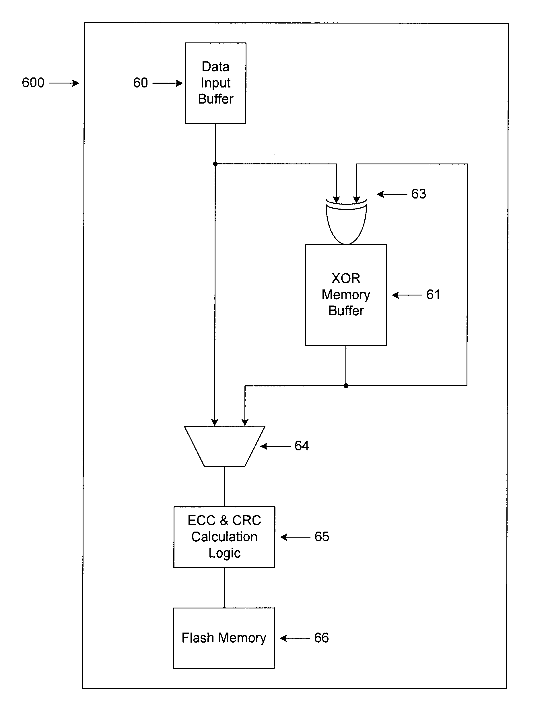
Image

Examples
Embodiment Construction
[0046]The figures described above and the written description of specific structures and functions below are not presented to limit the scope of what Applicants have invented or the scope of the appended claims. Rather, the figures and written description are provided to teach any person skilled in the art to make and use the inventions for which patent protection is sought. Those skilled in the art will appreciate that not all features of a commercial embodiment of the inventions are described or shown for the sake of clarity and understanding. Persons of skill in this art will also appreciate that the development of an actual commercial embodiment incorporating aspects of the present inventions will require numerous implementation-specific decisions to achieve the developer's ultimate goal for the commercial embodiment. Such implementation-specific decisions may include, and likely are not limited to, compliance with system-related, business-related, government-related and other c...
PUM
 Abstract
Description
Claims
Application Information