Electronic device

a technology of electronic devices and protective resins, applied in piezoelectric/electrostrictive device details, piezoelectric/electrostrictive/magnetostrictive devices, piezoelectric/electrostriction/magnetostriction machines, etc., can solve problems such as troublesome operation of removing and then reapplying protective resins formed on narrow places, and easy cracks in base substrates to achieve the effect of preventing

Inactive Publication Date: 2011-09-15
SEIKO EPSON CORP
View PDF3 Cites 9 Cited by
  • Summary
  • Abstract
  • Description
  • Claims
  • Application Information

AI Technical Summary

Benefits of technology

[0025]According to the configuration described above, it is possible to effectively prevent t...

Problems solved by technology

However, the operation of removing and then reapplying the protective resin formed on the narrow place will be troublesome...

Method used


Image

  • Electronic device
  • Electronic device
  • Electronic device

Examples


Embodiment Construction

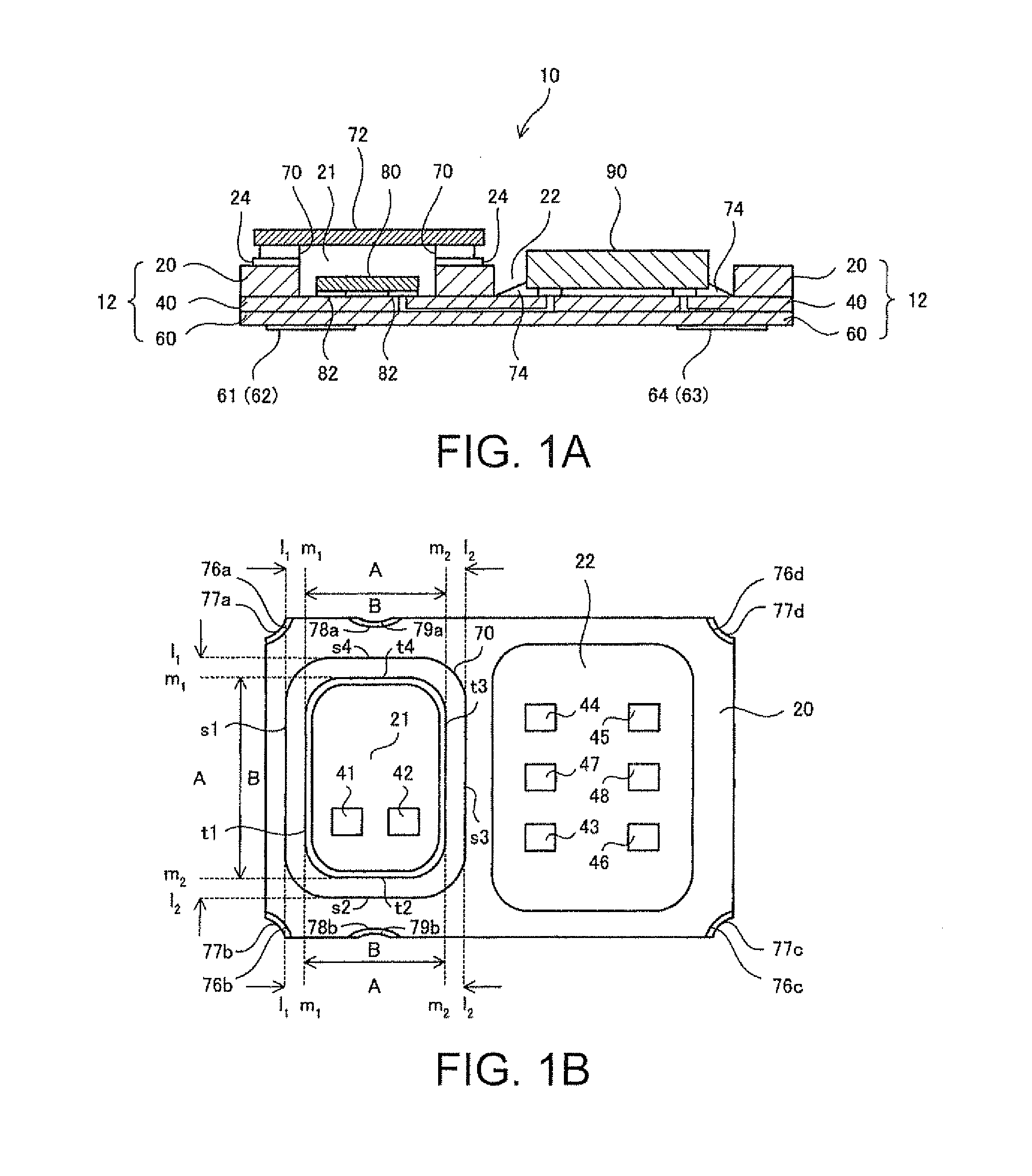
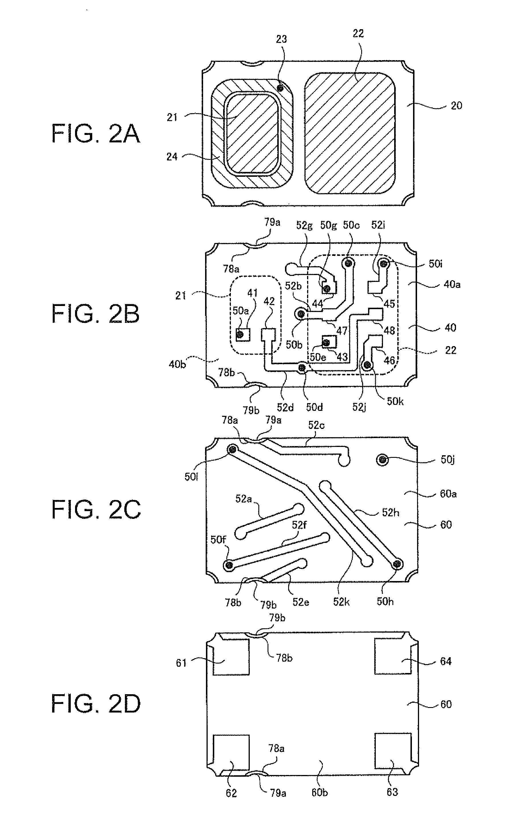
[0032]Hereinafter an electronic device according to an embodiment of the invention will be explained in detail with reference to the accompanying drawings. FIGS. 1A and 1B are diagrams showing a schematic configuration of the electronic device 10 according to the present embodiment. FIG. 1A shows a side cross-sectional view of the electronic device, and FIG. 1B shows a plan view (except lead electrodes) of the base substrate. As shown in the drawings, the electronic device 10 according to the present embodiment is composed of a resonator element 80, an IC chip 90, first through third substrates 20, 40, and 60 constituting the base substrate 12.

[0033]As the resonator element 80 to be mounted to the electronic device 10, a crystal resonator element such as a tuning-fork crystal resonator element can be used. It should be noted that the resonator element 80 can be an AT-cut crystal resonator element, an surface acoustic wave crystal resonator element, and so on besides the tuning-fork ...


PUM


Abstract

An electronic device includes: a base substrate having a resonator element fixed to one of principal surfaces, and provided with at least one lead wire; a frame member having a substantially rectangular shape, disposed on the one of the principal surfaces so as to surround a periphery of the resonator element, wherein side surface of the base substrate is provided with a side surface recessed section having a terminal electrically connected to the lead wire, and the side surface recessed section is disposed on the side surface of the base substrate on a side where the resonator element is fixed, at a position where at least a part of the side surface recessed section overlaps an area between two extended lines passing through respective outer side surfaces of the frame member opposed to each other in a plan view from the one of the principal surfaces of the base substrate.

Description

BACKGROUND[0001]1. Technical Field[0002]The present invention relates to an electronic device to be mounted to electronic apparatuses.[0003]2. Related Art[0004]Electronic devices having electronic components on a substrate are widely used for electronic apparatuses such as portable terminals or mobile phones. In accordance with downsizing and low-profiling of electronic apparatuses, downsizing and low-profiling are required for various types of electronic devices. In JP-A-2009-27465 (Document 1) there is disclosed an example of an electronic device achieving such downsizing.[0005]FIGS. 5A and 5B are cross-sectional view of a crystal oscillator described in Document 1 and plan view thereof except a cover, respectively. As shown in the drawings, the crystal oscillator according to Document 1 has a container main body 100 formed of a laminated ceramic composed of a bottom plate 100a and a frame wall 100b, the container main body 100 being provided with a recessed section 120 and a plan...

Claims


Application Information

Patent Timeline
IPC IPC(8): H01L41/04
CPCH03H9/0542H03H9/1021
Inventor CHIBA, SEIICHI
Owner SEIKO EPSON CORP
Why Eureka
Try Eureka